
Rogers materials explained · Datasheet interpretation
TC350 Plus laminate properties describe an RF circuit substrate, including its dielectric behavior, heat conduction and mechanical response. This guide explains how to read those entries without confusing a material test with a finished-circuit prediction. For fabrication requirements and quotations, go to the Rogers TC350 Plus PCB manufacturing page.
TC350 Plus is a ceramic-filled PTFE material reinforced by woven glass. Its process Dk reference is 3.50 ± 0.05, while Rogers separately lists design Dk 3.62. Typical dissipation factor is 0.0017 at 10 GHz, and Z-direction thermal conductivity is 1.24 W/(m·K). Use the attached method, conditions and construction context when turning these entries into a design model.
Read the property, method and limitation together
| Property reference | Method or context | What the number does not establish |
|---|---|---|
| Process Dk 3.50 ± 0.05 | Tolerance shown on product page; datasheet nominal 3.50, IPC TM-650 2.5.5.5 at 10 GHz | A universal effective permittivity or impedance tolerance |
| Design Dk 3.62 | Microstrip differential phase length; 10 GHz; C-24/23/50 | A guaranteed circuit resonance for arbitrary geometry |
| Typical Df 0.0017 | IPC TM-650 2.5.5.5; 10 GHz; 23°C and 50% RH | Total connector-to-connector insertion loss |
| Thermal conductivity 1.24 W/(m·K) | Z direction; ASTM D5470 | A component junction temperature or assembly power limit |
| Typical CTE X/Y/Z: 10/9/38 ppm/°C | IPC TM-650 2.4.41; −55°C to 288°C | A guaranteed dimension change or plated-hole lifetime |
| Typical-value notice | Datasheet distinguishes averages from specification values | Guaranteed acceptance limits for every delivered board |
Resonance sensitivity explorer
f₂ = f₁ × (L₁/L₂) × √(εeff₁/εeff₂). Hold geometry and coupling assumptions consistent. These are effective permittivities from a transmission-line model, not automatically the published bulk or process Dk. The calculation illustrates sensitivity rather than synthesizing a filter.
What TC350 Plus actually describes
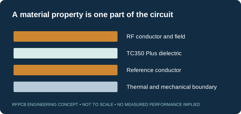
The TC350 Plus name identifies a Rogers laminate used to make printed circuits. Its composite contains a PTFE matrix, ceramic filler and woven-glass reinforcement. That composition matters when interpreting both electrical properties and processing instructions. It is not a thermoset resin system. Use the laminate name for the substrate specification and describe the function of the completed RF circuit separately.
The Rogers product overview places the material in applications where RF loss and thermal management matter together. Selecting a candidate from that description is only the beginning of design work. A board also has conductors, interfaces, mechanical features and operating conditions. Keep the full grade designation in your research notes, especially when comparing TC350 Plus with TC350 or another laminate. Similar names and similar nominal Dk values do not establish interchangeable composition, processing or circuit behavior.
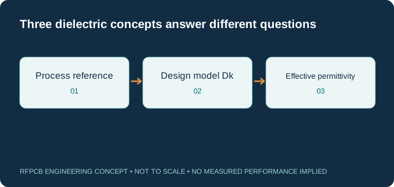
Why process Dk and design Dk differ
Process Dk is associated with a specified material test. Design Dk is a separate reference intended to support circuit modeling. Rogers explains the distinction in its discussion of dielectric-constant measurement: different measurement structures and techniques can produce different reported values. The TC350 Plus datasheet identifies microstrip differential phase length for its design entry, rather than using the process test method for both numbers.
The two values should therefore be labeled, not averaged. Subtracting them also does not reveal the manufacturing variation of a particular batch. When documenting a simulation, record which input was used, the reason it was selected and the geometry for which the model applies. If a previous design relied on measured calibration, preserve that evidence before replacing its model value with a number copied from a newer summary table. A consistent modeling basis is more useful than an unlabeled Dk field.
Effective permittivity belongs to the transmission line
A microstrip field occupies both dielectric and the region above it. Its propagation depends on the proportions of the field in those environments, so effective permittivity is a property of the guided structure. Trace width, substrate spacing and surrounding materials help determine it. Rogers discusses the differences among microstrip, coplanar and stripline structures in its transmission-line selection article.
This is why a calculator that asks for effective permittivity cannot automatically be filled with either published bulk Dk entry. First choose a model that represents the actual cross-section. Then use its effective value consistently for the frequency and geometry being explored. A solder mask, an enclosure boundary or a layer transition can require additional analysis. For a production transmission line, connect that model to defined dimensions and a suitable verification method rather than treating a simplified propagation estimate as artwork approval.
What a 10 GHz dissipation factor tells you
Dissipation factor describes dielectric loss under the specified test conditions. It is dimensionless, unlike insertion loss expressed in decibels. The TC350 Plus reference at 10 GHz does not directly supply attenuation per millimeter, and it does not say what an arbitrary board will lose between two connectors. Converting a material loss parameter into circuit behavior requires an electrical model with an actual field distribution and conductor system.
When comparing candidates, place test frequency and method beside each Df entry. Do not declare one finished board lower loss because a value measured at another frequency is smaller. A useful comparison also considers the route length, launches, conductor treatment and measurement reference planes. The RF PCB loss guide provides a practical way to divide those contributions. If measured data is available, describe the sample and test setup so the result can be connected to the construction being considered.
Thermal conductivity needs a direction and a heat path
The thermal-conductivity entry uses units of watts per meter-kelvin. The TC350 Plus datasheet identifies the Z direction, meaning through the thickness. This is different from thermal resistance, which describes a particular geometry and heat-flow arrangement. In the ideal one-dimensional slab model, resistance is thickness divided by conductivity times area: R = t/(kA). That relationship requires consistent units and uniform heat flow through the chosen area.
A real RF board rarely behaves as one isolated slab. Copper spreads heat, local sources create nonuniform temperatures, and mounting interfaces add their own resistance. Rogers' thermal-management discussion connects material selection with these circuit-level tradeoffs. Use the slab equation to understand the meaning of a property, not to assert a component temperature. A thermal prediction also needs dissipated power, mechanical boundaries, cooling conditions and the interfaces connecting the board to its surroundings.
Expansion data is different from electrical drift
Coefficient of thermal expansion describes dimensional response to temperature. The TC350 Plus datasheet provides separate X, Y and Z entries with a stated test interval. Those axes matter: a through-thickness expansion concern at a plated hole is not the same as in-plane alignment across a board. Keep the direction and temperature interval attached when transferring a value into an engineering worksheet.
Thermal coefficient of dielectric constant addresses a different phenomenon, the temperature dependence of dielectric behavior. Neither coefficient alone predicts the complete frequency drift of a resonator, because both physical dimensions and electrical properties can contribute. Fixtures, components and coupling can also change with temperature. If temperature stability is a requirement, use a model with appropriate temperature-dependent inputs and define a circuit-level test. Avoid converting a single summary coefficient into a broad environmental qualification claim without checking its conditions and the construction to which it applies.
Read thickness and copper as part of the property context
A laminate datasheet can list several core thicknesses and cladding configurations without making them electrically identical circuit implementations. Changing dielectric spacing usually changes the conductor dimensions needed for an intended impedance. It also changes the physical arrangement used in thermal and mechanical analysis. Review thickness, foil and geometry together rather than selecting one from a purchasing list after the RF layout is fixed.
The Rogers application-notes overview explains why copper surface roughness can influence both conductor loss and phase behavior. Consequently, comparing two prototypes with different foil or surface treatment may be comparing more than their dielectric materials. Label every changed factor in the test record. If a substitute construction is under consideration, the material selection guide can help organize those differences before a new model or prototype is approved.
Processing guidance explains why composition matters
The TC-series fabrication document linked from the TC350 Plus product page addresses filled, reinforced PTFE cores. It distinguishes hole-wall activation from adhesive desmear, and relates multilayer bonding to the chosen adhesive system. These are useful reminders that an electrical material selection also creates manufacturing questions. A familiar Dk does not mean a fabricator can simply apply an unrelated thermoset process unchanged.
For a design review, translate those questions into information the fabricator can evaluate: stackup, finished holes, registration-sensitive geometry and required inspection. Leave machine settings and treatment selection to a qualified process review using the relevant guidance and actual equipment. This article explains the material data; the TC350 Plus PCB manufacturing guide turns that information into an RFQ and acceptance package. Manufacturer processing recommendations support that review, but they do not establish a particular factory's approved limits or current material supply.
Explore resonance without confusing the input values
The resonance tool estimates how frequency changes when effective permittivity or electrical path length changes in an otherwise comparable structure. It uses f₂ = f₁ × (L₁/L₂) × √(εeff₁/εeff₂). With an illustrative 10 GHz baseline, unchanged 10 mm length and effective permittivity changing from 3.00 to 3.06, the result is approximately 9.9015 GHz, a decrease of about 0.985 percent.
Those effective values are hypothetical inputs, not reported TC350 Plus lot measurements. Do not enter process Dk as the baseline and design Dk as the changed value to claim a predicted manufacturing shift; that would mix two different measurement concepts. The tool also excludes coupling, fringing, temperature and detailed discontinuities. Use it to see which assumptions deserve closer attention. A filter or antenna still requires its actual geometry, operating environment and an appropriate electromagnetic model before the result can guide a layout decision.
Build a property record another engineer can follow
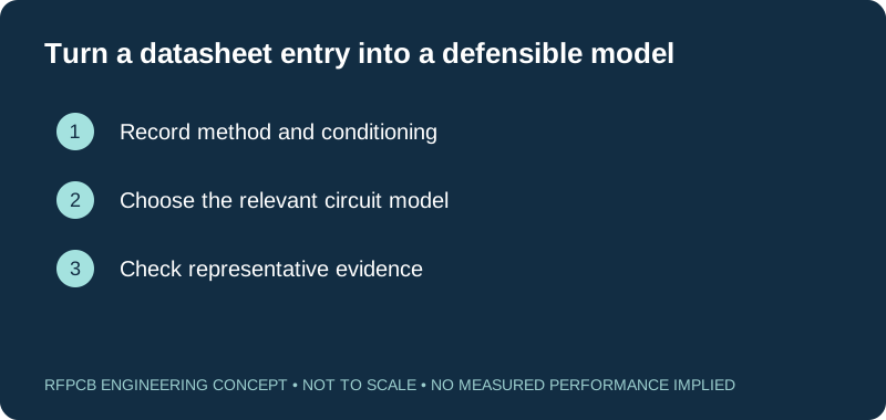
For each selected input, keep the manufacturer, exact grade, document revision, property name, units, test method and conditioning together. Add a note explaining where the value enters the design. Separate a typical reference from a requirement that must be satisfied by supplied material or by the completed circuit. The Rogers datasheet explicitly directs readers to the manufacturer for specification values rather than treating every typical entry as a guarantee.
Finish the record with the model version, construction assumptions and any supporting measurements. Mark unresolved items instead of silently filling them with a nearby material's properties. When a datasheet or supplier proposal changes, that record shows which calculations need review. Use the checklist below to capture readiness, then continue to the linked manufacturing page for a construction-specific inquiry. The result should be a traceable engineering argument from source property to circuit requirement, with the remaining uncertainty visible.
Prepare a reviewable engineering request
Check only the requirements you have actually documented. This list records readiness; it does not inspect your files or certify a design. Missing information is useful: identify it explicitly so the engineering review can resolve it before a production release.
These inputs are processed in your browser and are not submitted by this tool. The downloaded summary is a plain-text planning record. Use the secure quote form to send files; request an NDA first if your project requires one.
Manufacturing context
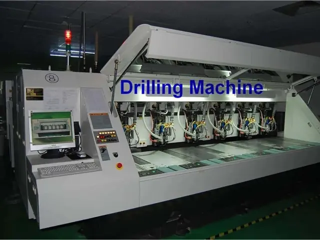
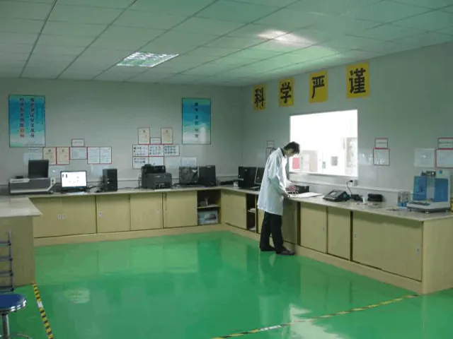
RFPCB and PCBSync share the manufacturing facility shown below. These process photographs illustrate the production environment; they are not evidence that a particular board, material grade or RF performance has been qualified. Request the documentation and inspection scope applicable to your project.

TC350 Plus laminate properties questions
Why do I see both 3.50 and 3.62 for TC350 Plus Dk?
They identify different references. Rogers lists 3.50 for process Dk and 3.62 for design Dk, with different measurement methods. Label each value and use the reference appropriate to the intended material or circuit-modeling task.
Is the 0.0017 Df value an insertion loss in dB?
No. Df is a dimensionless dielectric-loss parameter. Insertion loss describes a circuit path and also depends on its dimensions, conductors, launches and other structures. The two quantities cannot be exchanged without a suitable model.
Can this article be used to specify a maximum RF power?
No single maximum follows from these material entries. A power requirement needs the actual circuit, losses, duty, heat path and cooling conditions. Define temperature limits and verification conditions for the assembled design.
Where do I request a PCB made with TC350 Plus?
Use the Rogers TC350 Plus PCB manufacturing page to prepare a construction review. Attach the stackup, fabrication data, quantity and electrical or thermal acceptance requirements to the inquiry.
Continue your engineering review
Move from laminate data to a defined PCB
Continue to the TC350 Plus manufacturing guide for stackup, processing and quotation requirements. Carry your source references, model assumptions and acceptance goals into the project review.
Sources and engineering scope
- Rogers: TC350 Plus product overview and process/design Dk references
- Rogers: TC350 Plus laminate datasheet, composition, methods and typical properties
- Rogers: Managing PCB Materials Dielectric Constant (Dk)
- Rogers: Selecting Transmission Lines and Circuit Materials for Millimeter Waves
- Rogers: Optimizing Thermal Management for Wireless Communication Systems
- Rogers: High-Frequency Circuit Material App Notes, copper roughness and RF behavior
- Rogers: TC-series fabrication guidelines, including TC350 Plus
Manufacturer values apply to the identified grade, test method and construction. Engineering examples on this page are illustrative; they are not measured product results, inventory statements or certification claims. Manufacturer and product names belong to their respective owners. Keep the applicable datasheet revision with your approved manufacturing package.
Put this into production
Request a material, stackup and manufacturing review for your RF PCB project.