
Choose the right laminate
Compare the material family, frequency range, loss budget, thermal requirements and available thicknesses. Process Dk and design Dk serve different purposes.
Explore RF PCB materialsRFPCB.org supports RF PCB projects with material selection, hybrid stackup planning and manufacturing review. Explore Rogers, Taconic and PTFE options, define the electrical and inspection requirements, then request a quotation for your prototype or production build.
Start with the whole stackup. Dk, dielectric thickness, copper profile, finish and reference planes all affect the RF result. Illustration is conceptual.
Compare the material family, frequency range, loss budget, thermal requirements and available thicknesses. Process Dk and design Dk serve different purposes.
Explore RF PCB materialsSpecify reference planes, impedance, bond layers, copper and the via structure. Hybrid constructions need compatible materials and a reviewed lamination plan.
Plan a hybrid stackupIdentify critical dimensions, impedance coupons, required reports and the qualification plan before production. Match test scope to the application.
Review quality requirementsHydrocarbon ceramic laminate for RF designs. Review the correct Dk basis, available core and copper combination.
RO4350B PCB guideCompare its electrical properties and qualification requirements with your project specification.
RO4003C PCB guideGlass microfiber reinforced PTFE laminate. Consider dimensional control, handling and the manufacturing route.
RT/duroid 5880 guideEvaluate the exact grade; similar nominal Dk alone does not establish a drop-in material replacement.
Taconic PCB guideAlso explore RO3003, Arlon, Isola, Wangling F4B and PTFE PCB fabrication. Material availability and exact construction are confirmed during quotation.
| Parameter | What to provide | Review before release |
|---|---|---|
| Material and dielectric | Exact grade, thickness and relevant datasheet revision | Availability, Dk/Df test method and design assumptions |
| Layers and stackup | Copper layers, reference planes, bond layers and finished thickness | Symmetry, lamination compatibility and press thickness |
| Impedance | Target, tolerance, routing geometry and coupon requirements | Field-solver model, etch compensation and test method |
| Drilling and vias | Finished hole size, plating, blind/buried vias or back-drill needs | Aspect ratio, registration and residual stub limits |
| Copper and finish | Base versus finished copper, roughness requirement and finish | Loss, bondability, assembly compatibility and process limits |
| Inspection and delivery | Acceptance class, required reports, quantities and destination | Agreed test coverage, production schedule and shipping |
This is a quotation checklist, not a universal capability guarantee. Read the manufacturing capabilities guide and confirm limits against the specific construction.
Estimate a first-pass microstrip width and see how Dk and substrate thickness change the result.
Open impedance calculatorExplore a preliminary loss estimate with stated frequency and dielectric assumptions.
Estimate a loss budgetCompare laminate reference values alongside test conditions and links to material information.
Compare materialsUse conceptual layer arrangements to prepare a review. They require manufacturing approval.
Explore stackup concepts
Review material handling, drilling, plating and lamination requirements with the team.
See factory information
Features such as cavities, back-drilling and mixed materials need construction-specific checks.
Review cavity and back-drill needs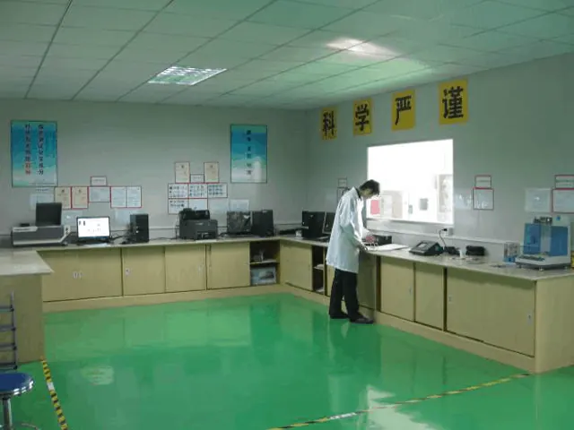
Request the inspection method and report scope relevant to your board, rather than assuming every test is included.
Plan inspection and reportingFactory photographs are shared with PCBSync, which the site owner identifies as the same factory. Equipment availability and project qualification must be confirmed.
Antennas, radar, communications and power amplifiers place different demands on the board. Begin with bandwidth, thermal load, loss budget, mechanical constraints and qualification requirements.
Explore RF applicationsAn RF PCB carries radio-frequency signals whose behaviour depends strongly on material properties, geometry and the return path. A suitable design controls transmission-line impedance, dielectric and conductor loss, coupling and manufacturing tolerances. Selecting a laminate is one part of the complete stackup and fabrication plan.
A hybrid construction can place RF material on selected layers and a different material in the rest of the stack. Lamination compatibility, thermal expansion, dielectric spacing and reliability requirements must be reviewed. See hybrid stackup PCB planning.
Only after reviewing the application's electrical, thermal, mechanical and qualification limits. Similar Dk or a brand cross-reference is not proof of equivalence. Use the candidate comparison tool, then validate the proposed construction.
Provide the material or electrical targets, dimensions, layers, quantity and delivery requirement. Add Gerber data, drill files, a fabrication drawing, impedance details and test requirements when available. You can start a request without a file and discuss an NDA first.
No. These tools support initial engineering decisions. Production dimensions require the selected laminate's design data, actual copper and dielectric thickness, the fabrication process and an agreed verification method.
Share your frequency, stackup, quantity and acceptance criteria. We will confirm material availability, review scope and a project-specific quotation.