In the ever-evolving world of electronics, the demand for high-frequency and high-speed applications has been steadily increasing. Radio Frequency (RF) and millimeter-wave circuits have become essential components in various industries, including telecommunications, aerospace, defense, and consumer electronics. Designing these circuits requires specialized knowledge and attention to detail, as even the slightest deviation can have a significant impact on performance.
This comprehensive guide aims to provide a practical approach to designing RF and millimeter-wave circuit Printed Circuit Boards (PCBs). By following the principles and techniques outlined in this article, engineers and designers will gain valuable insights into the intricacies of high-frequency circuit design, enabling them to create robust and efficient solutions.
Fundamentals of RF and Millimeter-Wave Circuit Design

Before delving into the design process, it is crucial to understand the fundamental principles that govern RF and millimeter-wave circuits.
1. Frequency Range
RF circuits typically operate in the frequency range of 3 kHz to 300 GHz, while millimeter-wave circuits operate at frequencies above 30 GHz, often extending into the terahertz range. These high frequencies present unique challenges in terms of signal propagation, interference, and electromagnetic compatibility.
2. Wavelength and Impedance Matching
At higher frequencies, the wavelength of the signal becomes shorter, making it more susceptible to electromagnetic interference and signal degradation. Proper impedance matching is essential to ensure efficient power transfer and minimize signal reflections, which can lead to unwanted resonances and signal distortion.
3. Skin Effect and Dielectric Losses
As the frequency increases, the skin effect becomes more pronounced, causing the current to flow primarily near the surface of the conductor. This phenomenon results in increased resistance and power dissipation. Additionally, dielectric losses in the PCB substrate material can contribute to signal attenuation and heating effects.
4. Electromagnetic Interference (EMI) and Shielding
High-frequency circuits are susceptible to EMI from external sources, as well as generating their own electromagnetic emissions. Proper shielding and grounding techniques are crucial to mitigate these effects and ensure compliance with regulatory standards.
PCB Design Considerations for RF and Millimeter-Wave Circuits

Designing PCBs for RF and millimeter-wave circuits requires careful consideration of various factors to ensure optimal performance and reliability.
1. PCB Material Selection
The choice of PCB material plays a critical role in the performance of high-frequency circuits. Some key factors to consider include:
- Dielectric constant (εr): Low dielectric constant materials are preferred to minimize signal propagation delays and reduce losses.
- Dissipation factor (tan δ): A low dissipation factor is desirable to minimize dielectric losses and ensure efficient power transfer.
- Thermal conductivity: High thermal conductivity materials help dissipate heat generated by high-frequency circuits, preventing degradation and failure.
Common PCB materials suitable for RF and millimeter-wave applications include Rogers RT/duroid, Taconic TLY, and various PTFE-based laminates.
2. Trace Geometries and Impedance Control
At high frequencies, the physical dimensions of the PCB traces become comparable to the wavelength of the signals, necessitating careful design of the trace geometries. Factors to consider include:
- Trace width and spacing: Appropriate trace widths and spacing must be calculated to achieve the desired characteristic impedance (e.g., 50 Ohms) and minimize coupling between adjacent traces.
- Discontinuities: Transitions, bends, and vias can introduce impedance discontinuities, leading to signal reflections and degradation. Proper design techniques, such as using mitred bends or compensated vias, can help mitigate these effects.
3. Grounding and Shielding Strategies
Proper grounding and shielding are essential for ensuring signal integrity and preventing electromagnetic interference in high-frequency circuits. Strategies include:
- Solid ground planes: Implementing continuous ground planes on one or more layers of the PCB provides a low-impedance return path for signals and improves shielding.
- Guard traces: Inserting grounded guard traces between high-frequency signal traces can help reduce coupling and crosstalk.
- Shielding enclosures: Using conductive enclosures or shielding cans can prevent external EMI from affecting the circuit and contain emissions from the circuit itself.
4. Layout Considerations
The physical layout of components and traces on the PCB can significantly impact the performance of high-frequency circuits. Some key considerations include:
- Component placement: Proper placement of active and passive components can minimize trace lengths, reducing signal attenuation and reflections.
- Routing: Signal traces should be routed with minimal bends and crossovers to maintain signal integrity and reduce parasitic effects.
- Isolation and partitioning: Separating high-frequency circuits from digital or low-frequency circuits can prevent unwanted coupling and interference.
- Thermal management: Proper placement of heat-generating components and adequate provision for heat dissipation (e.g., thermal vias, heat sinks) can prevent overheating and performance degradation.
5. Simulation and Verification
Before proceeding to fabrication, it is essential to simulate and verify the design using appropriate software tools. Electromagnetic (EM) simulation software, such as Ansys HFSS, Keysight ADS, or Cadence AWR, can provide accurate predictions of the circuit’s performance and help identify potential issues.
Manufacturing Considerations

Once the design is finalized, the next step is to ensure proper manufacturing techniques are employed to maintain the integrity of the high-frequency circuits.
1. Fabrication Tolerances
Tight fabrication tolerances are critical for RF and millimeter-wave circuits. Even small deviations in trace widths, spacing, or material properties can have a significant impact on performance. It is essential to work with experienced manufacturers who can consistently meet the required tolerances.
2. Surface Finish and Plating
The surface finish and plating of the PCB can affect signal propagation and dissipation. Common surface finishes for high-frequency circuits include Immersion Silver (ImAg), Electroless Nickel Immersion Gold (ENIG), and Hard Gold over Nickel.
3. Assembly and Soldering
Proper assembly and soldering techniques are crucial to ensure reliable connectivity and minimize parasitic effects. Techniques such as reflow soldering, ultrasonic soldering, or wire bonding may be employed, depending on the specific requirements of the circuit.
4. Testing and Validation
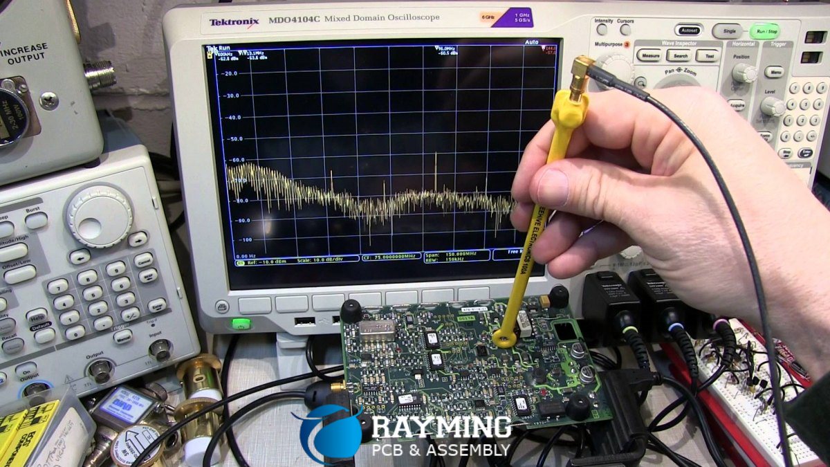
After manufacturing, it is essential to thoroughly test and validate the performance of the RF and millimeter-wave circuits. This may involve the use of specialized test equipment, such as vector network analyzers, spectrum analyzers, and signal generators, to measure parameters like insertion loss, return loss, and signal integrity.
Practical Design Example: Bandpass Filter
To illustrate the design process, let’s consider a practical example of designing a bandpass filter for an RF application.
1. Design Specifications
- Center frequency: 2.4 GHz (WiFi band)
- Bandwidth: 100 MHz
- Insertion loss: < 3 dB
- Return loss: > 15 dB
- PCB material: Rogers RO4003C (εr = 3.38, tan δ = 0.0027)
2. Filter Topology Selection
For this example, we will design a coupled-line bandpass filter using parallel-coupled microstrip lines. This topology offers a compact size, relatively wide bandwidth, and good selectivity.
3. Filter Design
Using filter synthesis techniques and industry-standard design tools (e.g., Keysight ADS, Cadence AWR), we can calculate the required coupling coefficients, line lengths, and spacing between the coupled lines to achieve the desired filter response.
4. Layout and Simulation
The calculated dimensions and parameters are then used to create the physical layout of the filter on the PCB. Electromagnetic simulation software, such as Ansys HFSS or Sonnet, can be employed to analyze the performance of the filter and optimize the design if necessary.
5. Fabrication and Testing
Once the design is finalized, the PCB can be fabricated using the appropriate manufacturing techniques and materials. After assembly, the filter should be thoroughly tested using a vector network analyzer to measure the insertion loss, return loss, and frequency response, ensuring compliance with the design specifications.
Frequently Asked Questions (FAQ)

- What is the difference between RF and millimeter-wave circuits? RF circuits operate in the frequency range of 3 kHz to 300 GHz, while millimeter-wave circuits operate at frequencies above 30 GHz, often extending into the terahertz range. Millimeter-wave circuits face additional challenges due to the shorter wavelengths and higher frequencies involved.
- Why is impedance matching important in high-frequency circuit design? Impedance matching is crucial for efficient power transfer and minimizing signal reflections, which can lead to unwanted resonances and signal distortion. Proper impedance matching ensures that the maximum amount of signal power is delivered to the load, improving overall circuit performance.
- What are the primary causes of signal loss in RF and millimeter-wave circuits? The main causes of signal loss in high-frequency circuits include skin effect, dielectric losses, conductor losses, and radiation losses. Skin effect causes the current to flow primarily near the surface of the conductor, increasing resistance and power dissipation. Dielectric losses occur in the PCB substrate material and can contribute to signal attenuation and heating effects.
- How does the choice of PCB material affect the performance of high-frequency circuits? The choice of PCB material significantly impacts the performance of RF and millimeter-wave circuits. Factors such as dielectric constant, dissipation factor, and thermal conductivity play crucial roles. Low dielectric constant materials with low dissipation factor and high thermal conductivity are preferred for high-frequency applications.
- What are some common techniques for shielding and grounding in high-frequency circuit design? Common shielding and grounding techniques include implementing solid ground planes, using guard traces between high-frequency signal traces, and employing conductive shielding enclosures or shielding cans. Proper grounding and shielding are essential for ensuring signal integrity and preventing electromagnetic interference.
By following the principles and techniques outlined in this practical guide, engineers and designers can confidently tackle the challenges of designing RF and millimeter-wave circuit PCBs, enabling the development of high-performance and reliable electronic systems for a wide range of applications.
Leave a Reply