
Put RF material where it matters.
A hybrid stackup combines different laminate systems within one PCB. Use a suitable RF dielectric around critical structures and a compatible construction for power, control and digital routing, with the full lamination system reviewed before release.
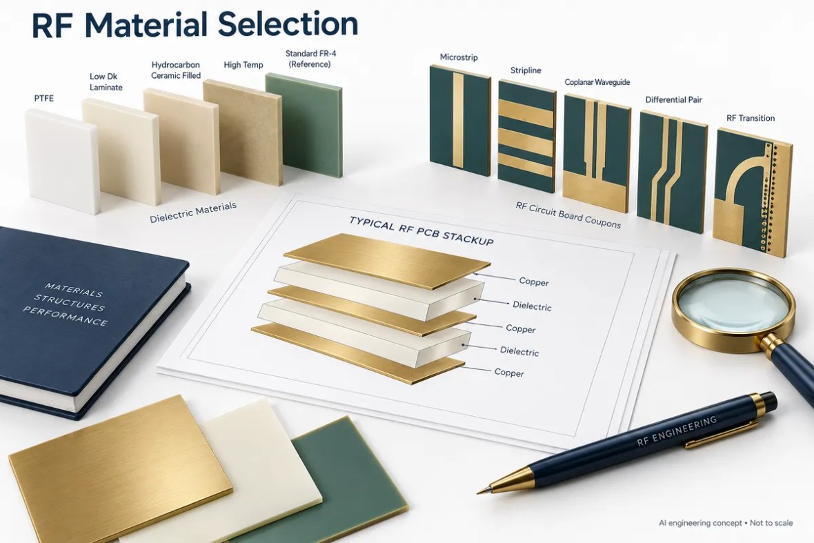
A hybrid stackup combines different laminate systems within one PCB. Use a suitable RF dielectric around critical structures and a compatible construction for power, control and digital routing, with the full lamination system reviewed before release. Review the build-specific requirements below and use the interactive tool to prepare better engineering questions.
What is a Rogers and FR-4 hybrid PCB?
A hybrid PCB uses more than one laminate family in the same bonded construction. In a typical RF project, selected layers provide the dielectric environment for microwave traces while other layers carry digital control, power and general interconnects. The design objective is a useful balance of electrical performance, board integration and manufacturing cost.
Hybrid does not mean that the non-RF dielectric can be ignored. Fields can extend through more than one region, particularly around transitions and complex transmission structures. Reference-plane placement and local geometry determine which dielectric properties affect a net. Begin by assigning signal functions to layers and then choose the materials surrounding each critical route.
Define the bonding system, not only the core names
A stackup is incomplete if it lists Rogers cores and FR-4 but omits the bonding layers. Specify candidate bondply or prepreg, cured thickness, copper weights and lamination sequence. The fabricator needs to review resin flow, copper fill, material conditioning, pressing compatibility and hole processing. A generic instruction to use standard FR-4 prepreg is not enough for every mixed-material construction.
Rogers publishes dedicated guidance on RO4000/FR-4 hybrid flatness and on its bonding materials. That guidance reinforces the need to consider the actual construction and processing route. It does not make all combinations interchangeable. Use the approved stackup drawing as the source of truth for quoting, fabrication and any later engineering change.
Three views of the engineering decision
Hybrid material-cost scenario
Compare material-only budgets using your own costs in the same currency and equal area/thickness basis.
Hybrid = RF cost × share + other cost × (1 − share) + allowance. Excludes fabrication, tooling, panel yield, test, shipping and margin. Share is material allocation, not copper-layer percentage.
Balance the structure and protect the RF reference
Review symmetry in dielectric construction, copper distribution and mechanical layout. An apparently symmetric layer count can still have an unbalanced copper pattern or material arrangement. Large cavities, dense copper on one side and local component heat can add further constraints. Bow and twist requirements should reflect the assembly process and product geometry.
Place a clear reference plane near the RF routing layer where the electrical architecture requires it. Keep return-path continuity explicit when a signal changes layer or crosses a connector interface. If several bonding cycles or unusual via structures are involved, ask how they affect registration, achievable tolerances and the inspection plan. The multilayer RF page explains the routing and manufacturing handoff.
When does a hybrid build reduce cost?
Using less premium laminate can reduce one cost component, but total board price also includes panel utilization, bonding materials, drilling, plating, inspection, scrap risk and setup. A simple all-RF board can sometimes be easier to manufacture than a highly asymmetric hybrid. Compare quotations for the same electrical and acceptance requirements before choosing.
The material-only scenario tool below lets you explore the arithmetic with your own costs. It deliberately does not invent supplier prices or convert copper-layer count into a laminate-volume estimate. Enter an RF material share based on a bill of materials or an agreed construction estimate. A final quotation needs the complete drawing and production quantity.
What the manufacturing review needs
| Review area | Define in your package | Confirm before release |
|---|---|---|
| RF core | Exact Rogers or alternative grade | Thickness, copper type and field region |
| Other core | Exact FR-4 or high-speed grade | Thermal and process compatibility |
| Bonding layers | Named bondply/prepreg system | Cured thickness and lamination sequence |
| Mechanical balance | Copper distribution and stack symmetry | Bow/twist and assembly needs |
These are review requirements, not universal capability limits. The order-specific drawing, process window and acceptance plan control the build.
Prepare a quotation that engineering can review
A useful RF PCB quotation starts with a controlled design package. Send Gerber or an agreed manufacturing format, NC drill data, a dimensioned outline, the board revision and a stackup drawing. Add quantity, delivery destination and the requested schedule. If some details are still open, mark them explicitly instead of letting a drawing, an email and a file name imply different requirements.
Separate mandatory requirements from preferences. A specified laminate, a customer-approved alternative and a request for a recommendation are three different purchasing instructions. State whether the supplier may propose changes to dielectric thickness, line geometry, panelization or finish, and who approves those changes. Changes that affect RF behavior should return to the design owner before release.
What affects the price?
Board area and panel utilization, quantity, material availability, stackup complexity, drilling and plating, special mechanical features, inspection and test all influence cost. Tight tolerances can also change the achievable yield and process route. An online estimate cannot account for every interaction in an unusual construction.
Use the panel and material cost tool to explore the assumptions it exposes, then request a reviewed quotation. Confirm tooling or setup charges, engineering changes, shipping, taxes and the included report package in the commercial offer.
What affects delivery?
Material stock, engineering clarification, special tooling, lamination cycles and the agreed inspection plan can affect the schedule. Assembly adds component procurement, stencil preparation, programming and fixture readiness. The requested date is a planning input until the supplier confirms the complete order scope.
The website’s response-time target describes enquiry handling. It is not a guarantee that a complex RF build can be priced, fabricated or delivered within the same period. Ask the team to identify the critical dependencies for your project.
From review to repeatable production
Agree the build
Engineering reviews material, geometry, mechanical features and test requirements. Open questions and proposed changes are documented. The approved drawing and stackup become the manufacturing baseline.
Verify the first build
Define which records are needed for the prototype: electrical test, impedance, dimensional inspection, cross-sections or an agreed RF measurement. Evaluate the evidence against the relevant acceptance criteria.
Control later changes
Keep revision, material substitutions, process changes and test updates traceable. A successful prototype is the starting point for production control, not permission to change the construction silently.
For a performance issue, retain the board revision, lot reference, measurement setup and operating conditions. Comparing repeatable measurements is more useful than comparing screenshots taken with different fixtures or calibration. Define the investigation and disposition with the supplier using the actual order requirements.
Is your hybrid stackup PCB package ready?
Select what is ready. This checklist runs locally and does not upload files or place an order.
The factory behind the engineering review
Use real process and laboratory evidence when qualifying a supplier. The photographs below come from the shared RFPCB / PCBSync facility archive. Discuss the equipment and inspection records relevant to your order through our quality page.



Hybrid Stackup PCB — Rogers + FR-4: common questions
Can any Rogers material be bonded with any FR-4 prepreg?
No. Compatibility depends on the exact laminate and bonding system, processing conditions and construction. Submit the proposed combination for review.
Are hybrid stackups always cheaper?
No. Premium-material savings may be offset by process complexity, yield, additional cycles or testing. Compare complete quotations.
Can the manufacturer change the stackup to improve yield?
Proposed changes should be documented and approved, especially where dielectric thickness or material affects impedance, phase or loss.
Continue the engineering review
Multilayer RF PCB Manufacturing
A multilayer RF PCB integrates microwave routing, reference planes, power and digital functions. The useful layer count is the one that supports the electrical architecture and a manufacturable stackup.
Controlled Impedance PCB Manufacturing
Controlled impedance PCB manufacturing turns a nominal electrical target into a reviewed geometry, material construction and measurement plan. Specify the controlled nets and acceptance window before fabrication begins.
High Frequency PCB Manufacturing
High frequency PCB manufacturing combines a suitable laminate with controlled geometry, return paths and an agreed test plan. Start with the operating band, loss budget and assembly environment, then choose a construction the factory can repeat.
Technical references and manufacturing scope
The engineering explanations distinguish ideal estimates from production acceptance. Use current material data and the approved drawing for the actual build. RFPCB and PCBSync share a manufacturing operation; the shared factory overview and rigid-board capability table provide context, while specific combinations require review.
- Rogers engineering tools and material calculations
- Rogers: RO4000 / FR-4 hybrid flatness
- Rogers: circuit materials and high-frequency losses
- Texas Instruments: AFE79xx layout and via-transition guidance
Engineering guide updated September 2026. Schematics illustrate concepts and are not fabrication-ready drawings. Product and material names belong to their respective owners.
Send the construction, not just the keyword.
Share your board revision, stackup, quantity and the requirements that matter. The team can identify open questions and confirm the manufacturing and test scope before quoting.
Ready for a quotation?
Send your requirements for a material, stackup and manufacturing review. Price and schedule are confirmed for your project.