
Useful tools.
Visible assumptions.
Explore material models, transmission-line geometry, stackup thickness and cost scenarios. Then carry the confirmed requirements into a fabrication review.
Start with a dedicated engineering resource
Use these published tools with their visible assumptions, source documents and manufacturing-review guidance.
PCB Impedance Calculator — Microstrip & Width Solver
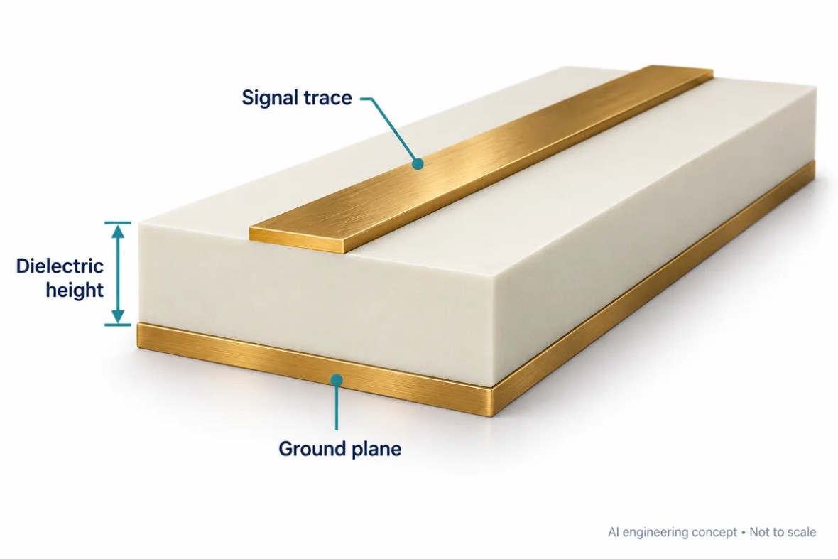
Calculate the ideal impedance of an isolated microstrip or solve for a target trace width. The result exposes its assumptions so you can take a useful starting geometry to manufacturing engineering.
Open resourceRF PCB Insertion Loss Calculator & Budget
Build a simple RF path budget from entered attenuation, or estimate the dielectric contribution of an ideal microstrip. Keep partial material estimates separate from a complete measured insertion loss.
Open resourceRF PCB Dk / Df Comparison Table
Search a curated table of RF laminate properties with direct manufacturer sources. Process Dk, design Dk and Df remain separate, with the conditions needed to interpret them.
Open resourceRF PCB Material Cross-Reference & Candidate Tool
Screen selected materials by reported Dk proximity and Df ceiling, then review the differences that determine whether a proposed change can work. The tool never treats a numerical match as replacement approval.
Open resourceRF PCB Stackup Library — 2, 4, 6 & 8 Layers
Explore four concept stackups, inspect the dielectric and copper schedule, and copy a nominal thickness summary. Use the example as a discussion document before the factory confirms a manufacturable construction.
Open resourceRF PCB Design Guide & Review Checklist
Use a practical sequence from requirements and material modeling to layout, manufacturing review and test. Build a project brief, copy the checklist and print the guide for your design review.
Open resourceFor quantity and material-cost scenarios, use the panel and cost explorer. Estimates use editable assumptions and are not live factory prices.
Quick engineering unit converter
Convert dimensions without mixing millimetres, mils and micrometres. One mil is exactly 0.0254 mm.
Use an estimate for the right purpose
Impedance is a geometry model
The available microstrip calculator is quasi-static and assumes zero copper thickness, no solder mask and an isolated trace over a continuous ground plane. It does not represent coplanar waveguide, differential pairs or the entire RF launch.
Use an appropriate field solver and the approved manufacturing stackup for production dimensions.
Loss needs a complete path model
Df contributes to dielectric loss. Copper roughness, conductor geometry, finish, vias and connectors also contribute to measured attenuation. A generic Df comparison cannot predict complete circuit insertion loss.
Define frequency, reference planes and fixture treatment before comparing measurements.
Cost is construction-specific
Example rates are editable assumptions. Panel yield and setup affect effective unit cost, but the accepted grade, foil, tests and delivery requirement determine a reviewed quotation.
Compare quotes on the same scope and keep approved substitutions explicit.
Source conditions belong with the number
Retain frequency, test method, construction and document revision beside material values. Keep process Dk separate from design Dk when the manufacturer supplies both.
For a source discrepancy, request model confirmation rather than averaging conflicting values.
Build a useful engineering handoff
Select what is ready. This checklist runs locally and does not upload files or place an order.
Ready to replace estimates with a build plan?
Attach the engineering package and highlight the assumptions that still need confirmation. The review can then address the material, process and acceptance requirements together.
Related engineering decisions
Related engineering decisions
In this section
Dk / Df Comparison Table
View pageImpedance Calculator
View pageInsertion Loss Calculator
View pageMaterial Cross-Reference Tool
View pageRF PCB Design Guide & Checklist
View pageRF PCB DFM Checklist
View pageRF PCB Laminate Datasheets & Manufacturer References
View pageRF PCB Stackup Library
View pageRF PCB Test Report Guide
View pageReady for a quotation?
Send your requirements for a material, stackup and manufacturing review. Price and schedule are confirmed for your project.