
RF MATERIAL ENGINEERING / DESIGN TO QUOTATION
Select the exact Taconic laminate, test conditions and copper construction.
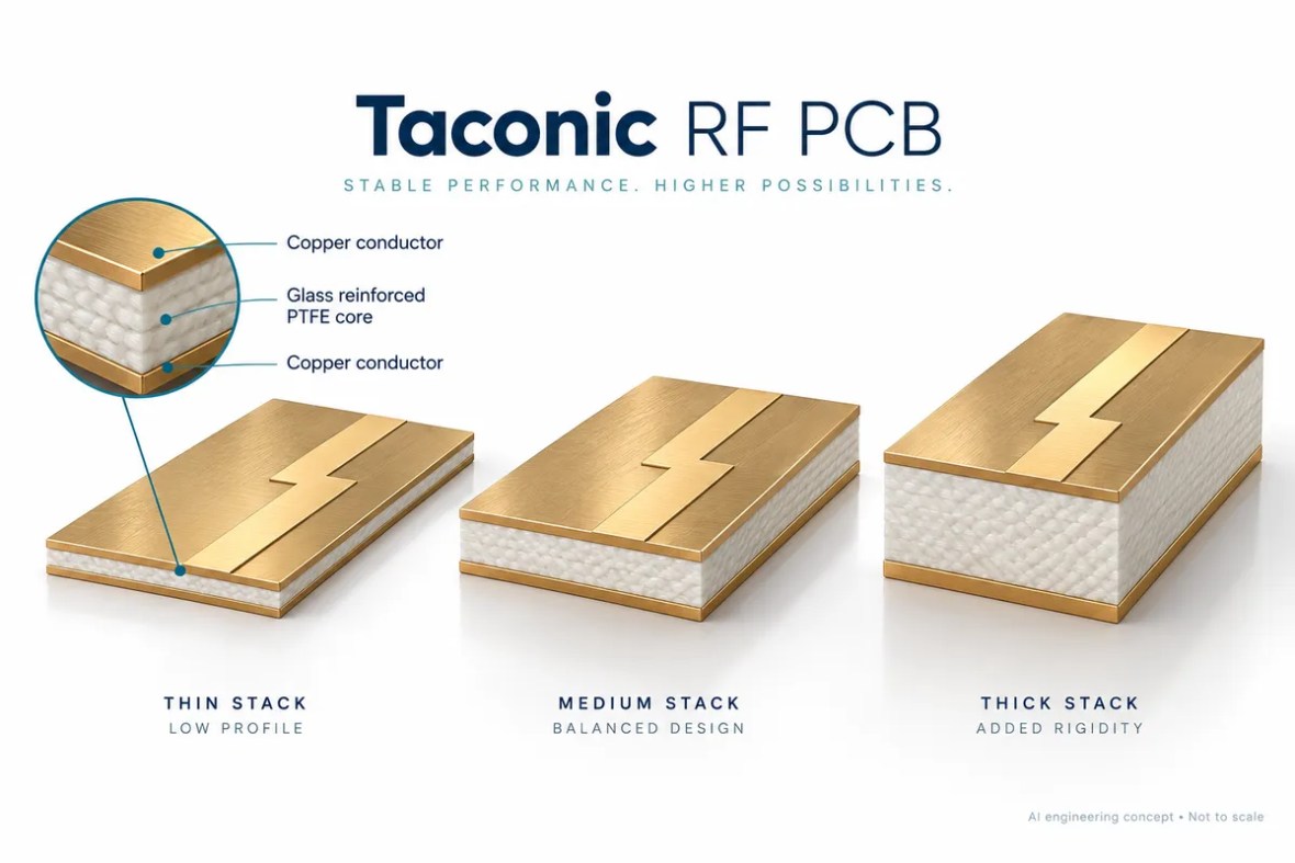
Taconic PCB describes boards made with a family of RF laminate products, not one universal dielectric. A useful specification starts with the exact grade, such as TLY-5, and continues with dielectric thickness, copper and verification requirements. AGC acquired the Taconic advanced dielectric division in 2019; current documentation should be checked by product and revision. This guide helps engineers compare qualified constructions and helps buyers prepare an RFQ without assuming all Taconic materials have identical electrical or processing properties.
Taconic PCB: material data and model assumptions
| Property or grade | Published value / description | Conditions and interpretation |
|---|---|---|
| TLY-5 | Dk 2.20 ± 0.02; Df 0.0009 | 10 GHz; woven fiberglass/PTFE |
| RF-35 historical reference | Dk 3.50; Df 0.0018 | 1.9 GHz; woven glass/ceramic/PTFE |
| RF-35 suffix variants | Confirm exact product | RF-35TC and other suffixes are separate constructions |
| Availability | Quotation confirmation required | A datasheet does not establish stock or lead time |
Values above are material references, not guaranteed finished-board performance. Consult the linked manufacturer document and confirm its revision for procurement. Source review: 24 September 2026.
Engineering decisions for Taconic PCB
Choose a grade before comparing suppliers
A purchase request that only says Taconic PCB leaves important engineering decisions unresolved. Identify the full laminate designation and approved construction before comparing quotations. TLY-5 is a glass-reinforced PTFE candidate for low-Dk RF structures, while other product families use different filler systems and target different tradeoffs. Ask a supplier to state the exact offered grade rather than accepting a generic equivalent. Keep the datasheet revision with the stackup drawing so subsequent builds can be checked against the same requirements.
Compare Dk and Df at their published conditions
The TLY-5 datasheet reports a nominal Dk of 2.20 and a dissipation factor of 0.0009 at 10 GHz. Historical RF-35 data commonly report 3.50 and 0.0018 at 1.9 GHz. A lower listed Df at one frequency does not establish a universal finished-circuit advantage over a value measured elsewhere. Compare the candidate materials under relevant, comparable conditions, then include conductor roughness and geometry. Where no verified design Dk is supplied, document and validate the chosen simulation assumption.
Thickness, foil and RF acceptance
An antenna feed network needs more than a nominal dielectric constant. Specify dielectric thickness tolerance, finished copper, conductor dimensions and the intended finish. Check how the RF geometry connects to components, plated holes and board-edge launches. If phase tracking or passive intermodulation matters, define a measurement method and acceptance limit for the finished structure. The brand name and foil description alone do not certify PIM performance. Use coupons or representative structures that include the features most likely to affect the product.
Manage legacy designs and alternatives
Legacy Taconic drawings may reference a grade or revision that requires a current supply check. Request written identification of the offered material and review changes in foil, thickness or bonding products. Do not infer current availability from an archived datasheet, and do not assume every product with an additional suffix is interchangeable. If an alternative is needed, compare geometry and loss budgets before ordering. Qualify the new stackup with relevant electrical and manufacturing evidence, then update the approved procurement description.
Real RF board references
The following photographs are from the RFPCB site archive. They show manufactured RF structures and hybrid boards. They are visual manufacturing references, not proof that every pictured board uses the material discussed on this page.


Taconic PCB design and cost tools
Adjust assumptions, compare scenarios and build a clear enquiry. Calculations run in your browser. Grade presets only change the Dk input; they do not set material prices, certify a construction or select a manufacturing process.
Taconic PCB budget & panel calculator
Editable example assumptions. USD. Not a factory price list.
Microstrip impedance & target-width solver
Editable grade presets. Confirm the design model; dimensions in millimetres.
Nominal stackup thickness planner
Separate RF dielectric, other dielectrics and copper.
Design workflow: from Dk to a manufacturable line
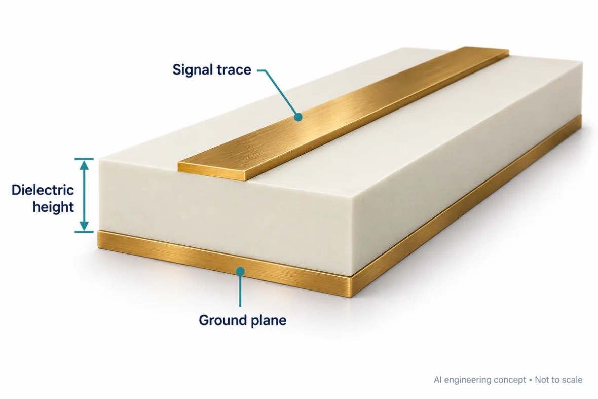
Begin with the distance from the RF trace to its reference plane, not the total finished-board thickness. Enter that dielectric height in millimetres and choose the dielectric constant appropriate to the confirmed material model. In target mode, the calculator solves a width for the requested impedance. In analysis mode, it estimates impedance from a width you enter. Change one assumption at a time to understand which dimensions are sensitive before committing the layout.
The solver uses a zero-copper-thickness Hammerstad–Jensen quasi-static microstrip approximation. It represents an isolated, uncoated trace over a continuous ground plane. It does not include solder mask, finite copper thickness, roughness, frequency dispersion, neighboring traces, coplanar grounds, via fences or connector launches. Frequency changes the wavelength output, while this model’s impedance remains quasi-static. A production field solver and a fabricator-approved stackup are needed for final controlled-impedance dimensions.
Use the delay and quarter-wavelength outputs as early electrical-length estimates. They do not replace a filter or antenna simulation. Resonant structures also respond to discontinuities, fringing fields, enclosure proximity and fabrication tolerance. For a sensitivity check, vary dielectric height and Dk over the confirmed tolerances and compare the resulting trace widths. Keep those ranges with the drawing instead of reporting a calculated width with unrealistic manufacturing precision.
Plan the stackup as a complete construction
The thickness planner adds the total selected RF dielectric, all other pressed dielectrics and equal copper thickness for each layer. Enter every core, bondply and prepreg contribution exactly once. For two copper layers, the model uses only the RF dielectric and copper. The output excludes solder mask and surface finish. It is a nominal arithmetic budget, not a prediction of resin flow, press shrinkage or an approved multilayer construction.
Before fabrication, ask for the actual layer sequence, material identifiers, pressed dielectric thicknesses, copper weights and tolerances. Review whether reference planes remain continuous beneath critical routes. Identify any blind, buried or through-hole transitions that need separate electrical or reliability evaluation. A total thickness that fits a connector does not by itself establish impedance, bond compatibility or layer balance. Review those requirements together with the proposed manufacturing process.
Cost and quotation: expose the assumptions
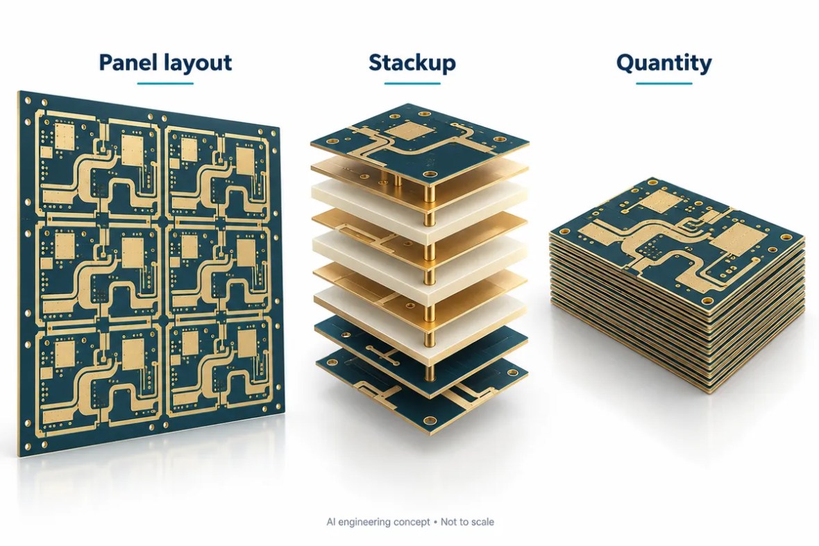
A useful early budget shows what drives the number. Board outline, usable panel size, spacing, ordered quantity and expected yield determine how many full panels the example allocates. The calculator compares a uniform zero-degree layout with a uniform ninety-degree layout and uses the better result. It does not perform mixed-orientation nesting, optimize irregular outlines or reserve tooling rails and coupons automatically. Enter the usable area after those manufacturing reservations.
Material cost is the amount allocated to all laminate in one usable panel. Fabrication cost applies to every board position started on the allocated panels, while testing cost applies to the ordered quantity. Setup is added once. These assumptions deliberately remain visible and editable. The displayed dollar figure is a scenario based on your inputs, not a live supplier price, availability statement or purchasing commitment. Shipping, taxes and assembly are excluded.
For a fair quotation comparison, hold the material grade, foil, stackup, finish, quantity, tolerances and tests constant. A low unit price may cover a different inspection plan or construction. Record any acceptable alternatives explicitly and request approval before substitution. Compare prototype and production quantities separately because setup allocation and panel utilization can change the effective unit cost. Enter confirmed supplier rates when available and rebuild the summary after changing the design.
What a complete RFQ should include
Send the fabrication data, NC drill, board outline and revision together with a layer-by-layer stackup. Include the manufacturer and exact laminate grade, dielectric thickness and tolerance, copper type, finished copper, finish and material substitution restrictions. Identify controlled-impedance nets and target tolerances. State whether the project also needs insertion loss, return loss, phase or other RF acceptance measurements, because these are separate deliverables with their own fixtures and coupons.
Specify the order quantity, panel preferences, delivery destination and required schedule. If the design is still evolving, identify which dimensions or materials remain open to engineering review. The summary button below collects valid calculator scenarios into editable text; it does not transmit your design or submit an order. Review that text, attach the actual manufacturing package and use the quotation form for a build-specific response.
Taconic PCB questions
Which Taconic material should I specify?
Specify the exact product and construction. TLY-5 is one documented option; a generic Taconic label cannot define Dk, Df, thickness, foil or current availability.
Can I compare TLY-5 and RF-35 by their Df numbers alone?
No. The cited values use different frequencies, and circuit loss also depends on copper, geometry and transitions. Use comparable data and a complete circuit model.
Is the online cost result a formal quotation?
No. It uses editable illustrative rates and a simplified panel model. A formal quotation requires the fabrication files, exact material construction, testing, quantity and delivery requirements.
Can I manufacture the calculated trace width directly?
Use it as an initial estimate. The model excludes finite copper thickness, mask and other production details. Agree final dimensions and tolerance with the fabricator using the approved stackup and appropriate field solver.
Compare related material choices
Continue the selection using the pages most relevant to the alternative construction: Wangling F4B PCB, PTFE / Teflon PCB, RF PCB Material Selection Guide. For thermoset RF alternatives, review RO4003C PCB and RO4350B PCB with their own design data and manufacturing requirements.
Material sources and scope
Manufacturer references support the material facts above. Engineering guidance and calculator scenarios are preliminary aids. No stock, lead time, certification, substitution or RF acceptance result is implied by the illustrations or example calculations.
Turn your Taconic PCB design into a clear RFQ
Use the button below to collect the current valid calculator scenarios into editable enquiry text. Attach your manufacturing files separately and review the assumptions before submitting. No calculator input is sent by this button.
- Gerber or agreed fabrication data, NC drill, outline and revision.
- Board quantity, panel requirements and delivery destination.
- Layer-by-layer stackup, material restrictions and copper requirements.
- Target impedance, tolerances, surface finish and test expectations.
- Required lead time and any acceptable engineering alternatives.
Related engineering decisions
Ready for a quotation?
Send your requirements for a material, stackup and manufacturing review. Price and schedule are confirmed for your project.