
Align the radio, feed network and production build.
A base station PCB can combine RF distribution, amplification, power and control. Define the board function, operating band and environmental requirements before choosing a material or a production process.
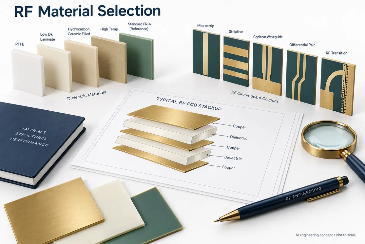
A base station PCB can combine RF distribution, amplification, power and control. Define the board function, operating band and environmental requirements before choosing a material or a production process. Use the application-specific review below to identify the information needed for material selection, fabrication and acceptance.
Define which part of the base station the board serves
A radio unit, antenna feed board, power amplifier and digital control board have different electrical priorities. Some assemblies combine several functions; others distribute them across modules. Identify the actual function, interfaces and expected production scope so the manufacturing review addresses the relevant constraints.
Describe the operating bands, channel configuration, output power, routing architecture and mechanical envelope. A general statement that the board is for 5G does not define the bandwidth, transmission structure or environmental conditions. Separate the RF-critical regions from general control and power routing while keeping their interactions visible.
Manage feed loss and channel consistency
A passive feed network reduces delivered power through conductor, dielectric, connector and other losses. In repeated channels, differences in loss and phase can matter as much as the average value. Use consistent reference planes to compare channels and account for the actual assembly condition.
The attenuation tool below calculates the power ratio associated with a stated matched-path insertion loss. It does not predict loss from a laminate datasheet. Enter a measured value or a justified model result at the relevant frequency. A loss term that already includes a connector or cable should not be added a second time elsewhere in the system budget.
Understand the application interfaces
Feed-path loss to delivered power
Convert an entered insertion loss into a matched-path power ratio. Use measured or justified modeled loss at the required frequency.
Pout = Pin × 10^(−loss / 10). Matched passive-path assumption. Missing delivered power is not necessarily all heat; reflection or radiation may contribute. No material-loss prediction is performed.
Select the construction for electrical and production needs
Appropriate RO4350B, RO4003C, Taconic or other materials can be evaluated against the design requirements. The grade, thickness, foil and finish must remain specific. There is no single laminate that is automatically optimal for every base-station board.
A hybrid RF and FR-4 stackup can be considered for integrated radio and control functions. Review bonding materials, copper balance and the local dielectric around controlled routes. For high-power sections, connect the design to the thermal and heavy-copper review rather than assuming a generic board thickness will satisfy cooling needs.
Define environmental and repeat-order controls
The installation environment may impose temperature, moisture, vibration or other requirements. State the applicable test plan, enclosure assumptions and acceptance criteria rather than relying on an outdoor or telecom label. Low passive intermodulation, when relevant, is a system and measurement requirement that needs its own definition.
For repeat production, maintain the approved material construction, RF geometry and test setup under change control. Component substitutions, finishes or connector changes can affect an assembled radio even if a bare-board continuity test passes. Define the required lot records and representative RF evidence through the quality review.
Application-to-manufacturing review
| Area | Define for the application | Confirm before release |
|---|---|---|
| Board role | Feed, radio, amplifier, power or control | Interfaces and channel architecture |
| Electrical budget | Band, loss, phase and power | Reference planes and relevant RF metrics |
| Construction | Exact materials and copper/finish schedule | Process and assembly compatibility |
| Production | Quantity, environment and repeat-order needs | Traceability and approved change process |
Connect these requirements to the Hybrid Stackup PCB — Rogers + FR-4 workflow. The approved stackup, drawing and order-specific acceptance plan define the build.
Build the acceptance plan around the application
Decide what the bare board must demonstrate and what belongs to the assembled product. Continuity testing, an impedance coupon, a calibrated RF network measurement and an installed-system test are different forms of evidence. None should silently stand in for another. Identify the required report, coverage, limits and review responsibility before the quotation is accepted.
Record the test configuration alongside the result: board revision, material construction, fixture, calibration, firmware or device settings, temperature and the relevant operating point. When comparing prototypes, keep these conditions consistent or explain the difference. A changed connector, cable or reference plane can make an apparent board improvement difficult to interpret.
For production, agree how first-article findings become controlled manufacturing requirements. Identify which dimensions and material choices are critical, what may be adjusted by engineering, and which changes require renewed validation. A repeat order should reference the approved revision and test plan rather than rely on a previous email description.
Visit quality and test evidence for supplier qualification and reporting questions. Where a customer program requires certificates or sector-specific approval, request the actual documents and applicable scope. An application example is not a product certification or a substitute for the customer’s acceptance process.
Prepare a quotation that engineering can review
A useful RF PCB quotation starts with a controlled design package. Send Gerber or an agreed manufacturing format, NC drill data, a dimensioned outline, the board revision and a stackup drawing. Add quantity, delivery destination and the requested schedule. If some details are still open, mark them explicitly instead of letting a drawing, an email and a file name imply different requirements.
Separate mandatory requirements from preferences. A specified laminate, a customer-approved alternative and a request for a recommendation are three different purchasing instructions. State whether the supplier may propose changes to dielectric thickness, line geometry, panelization or finish, and who approves those changes. Changes that affect RF behavior should return to the design owner before release.
What affects the price?
Board area and panel utilization, quantity, material availability, stackup complexity, drilling and plating, special mechanical features, inspection and test all influence cost. Tight tolerances can also change the achievable yield and process route. An online estimate cannot account for every interaction in an unusual construction.
Use the panel and material cost tool to explore the assumptions it exposes, then request a reviewed quotation. Confirm tooling or setup charges, engineering changes, shipping, taxes and the included report package in the commercial offer.
What affects delivery?
Material stock, engineering clarification, special tooling, lamination cycles and the agreed inspection plan can affect the schedule. Assembly adds component procurement, stencil preparation, programming and fixture readiness. The requested date is a planning input until the supplier confirms the complete order scope.
The website’s response-time target describes enquiry handling. It is not a guarantee that a complex RF build can be priced, fabricated or delivered within the same period. Ask the team to identify the critical dependencies for your project.
From review to repeatable production
Agree the build
Engineering reviews material, geometry, mechanical features and test requirements. Open questions and proposed changes are documented. The approved drawing and stackup become the manufacturing baseline.
Verify the first build
Define which records are needed for the prototype: electrical test, impedance, dimensional inspection, cross-sections or an agreed RF measurement. Evaluate the evidence against the relevant acceptance criteria.
Control later changes
Keep revision, material substitutions, process changes and test updates traceable. A successful prototype is the starting point for production control, not permission to change the construction silently.
For a performance issue, retain the board revision, lot reference, measurement setup and operating conditions. Comparing repeatable measurements is more useful than comparing screenshots taken with different fixtures or calibration. Define the investigation and disposition with the supplier using the actual order requirements.
Prepare your base station PCB enquiry
Select what is ready. This checklist runs locally and does not upload files or place an order.
Real manufacturing and laboratory context
These photographs are from the shared RFPCB / PCBSync facility archive. They show manufacturing and laboratory areas, not a claim that a pictured item is a certified base station PCB product. Review the actual process and report requirements with the team.



Base Station RF PCB Manufacturing: common questions
Is a base-station PCB always a high-frequency laminate board?
No. The function and signal requirements determine the material. A control board and an RF feed board can need different constructions.
Does the loss tool predict insertion loss from Df?
No. It converts an entered insertion loss into a power ratio and output power under a matched-path assumption.
Can low PIM be guaranteed from the laminate name?
No. Define the assembly, materials, contacts and measurement conditions relevant to the actual low-PIM requirement.
Related application decisions
5G & mmWave PCB Manufacturing
A 5G or millimeter-wave PCB brings RF interconnects, antenna structures and digital control into a tightly coupled design. Select the stackup around the actual operating band and bandwidth rather than the 5G label alone.
Antenna PCB Design & Manufacturing
An antenna PCB must preserve the radiator geometry, feed network and surrounding electromagnetic environment. Review the laminate, reference planes, enclosure and measurement method together before manufacturing.
RF Power Amplifier PCB Manufacturing
An RF power amplifier PCB supports the signal path, bias network and heat-removal structure. Review electrical loss, assembly interfaces and operating conditions together to turn a device-level design into a repeatable board.
Technical references and scope
Use current component and material documentation together with the approved design. The sources below provide engineering context; the specific product and manufacturing acceptance requirements remain project-dependent.
- Rogers wireless infrastructure material context
- Analog Devices base-station amplifier control
- RFPCB material selection and engineering tools
- Manufacturing capability review
Engineering guide updated September 2026. Diagrams are conceptual and not production drawings. Calculations are estimates under the stated assumptions.
Bring the application requirements into the quote.
Send the operating band, board revision, stackup, quantity and acceptance needs. The team can identify missing information and review the proposed manufacturing scope.
Ready for a quotation?
Send your requirements for a material, stackup and manufacturing review. Price and schedule are confirmed for your project.