
Material families · Practical selection
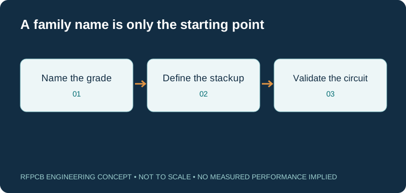
PTFE vs hydrocarbon PCB laminates compares broad material families. Start with a named grade, reinforcement, copper foil and stackup; a resin-family label is not a complete RF design model or purchasing specification.
PTFE-based and hydrocarbon/ceramic thermoset laminates can both serve RF circuits. Their exact grades differ in electrical behavior, reinforcement, mechanical properties and fabrication requirements. Select a specific construction against loss, dimensional, thermal and qualification requirements instead of choosing a family by slogan.
Questions to ask when comparing the two families
| Requirement | PTFE-based candidate | Hydrocarbon/ceramic candidate |
|---|---|---|
| Grade definition | Pure or reinforced/filled PTFE variants differ | Reinforcement and filler depend on exact product |
| Electrical model | Use grade, thickness and foil-specific references | Use grade, thickness and foil-specific references |
| Hole preparation | Confirm a qualified PTFE-compatible process | Confirm the applicable thermoset process |
| Bonding | Approve bondply/prepreg and pressed thickness | Approve compatible bonding system and press plan |
| Cost decision | Include processing, panel allocation and yield assumptions | Include processing, panel allocation and yield assumptions |
| Acceptance | Material identity plus agreed board/circuit tests | Material identity plus agreed board/circuit tests |
Guided wavelength and size explorer
λg = c / (f × √εeff), with c = 299.792458 mm·GHz. Use the effective value of your actual geometry. Quarter wavelength excludes fringing, loading, dispersion, coupling and end corrections. It is not production-ready artwork.
Separate resin, reinforcement and finished construction
PTFE is a polymer family, while an RF laminate can combine that resin with fillers or reinforcement to achieve particular properties. Hydrocarbon/ceramic thermoset products also differ from one another. Treat these descriptions as the start of a selection process, not as a complete bill of materials.
The board you buy also includes copper foil, bonding materials, plated features and a surface finish. Those elements can affect loss, dimensions and manufacturing yield. Ask for an exact manufacturer and product designation for every important dielectric region, together with the relevant thickness and copper specifications.
Avoid assigning one Dk or Df to an entire family
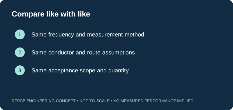
A family-level comparison cannot responsibly give one electrical number for every PTFE or hydrocarbon laminate. Use the current manufacturer document for the actual candidate and retain its frequency, test method and construction notes. Apparent differences between tables can result from different measurement conventions rather than a meaningful advantage in your circuit.
The Dk and Df comparison resource helps organize candidate data. It should support a documented selection, not replace the detailed material model used for a critical transmission line, resonator or antenna feed.
Choose by path loss and electrical length
A short interconnect and a long distributed network can place very different demands on a substrate. Identify the length of the sensitive path, operating band and loss budget. Consider whether mismatch at transitions or distributed line loss is likely to dominate before spending time comparing small differences in laminate data.
The wavelength explorer shows how effective permittivity changes the electrical scale of a circuit. It does not tell you that a particular laminate is suitable, and the calculated quarter wavelength is not a fabrication-ready resonator length. Geometry, field distribution and end effects still require engineering analysis.
Review holes and metallization with the selected material
A qualified fabrication route includes drilling or laser formation, surface preparation and metallization compatible with the chosen construction. Ask how the proposed hole structures interact with laminate thickness and any sequential processing. Do not transfer a generic hole-size claim from one material system to another without review.
If the design includes blind vias, buried vias or filled microvias, provide a layer-pair drawing. The HDI RF PCB guide explains why dielectric depth, landing geometry and the process sequence matter together. A single minimum diameter does not define the complete capability.
Check mechanical behavior and dimensional stability
RF performance can depend on geometry that changes during fabrication, assembly or use. The relevant concerns include dimensional compensation, thermal expansion, copper distribution and the interaction with housings or connectors. Different reinforced or filled grades can behave differently even when they share a resin family.
Identify the dimensions that are functionally critical and agree how they will be measured. For a board attached to a metal carrier, include the attachment and operating conditions in the review. A material datasheet alone cannot predict the mechanical behavior of the completed assembly.
Make the bonding system part of the RF model
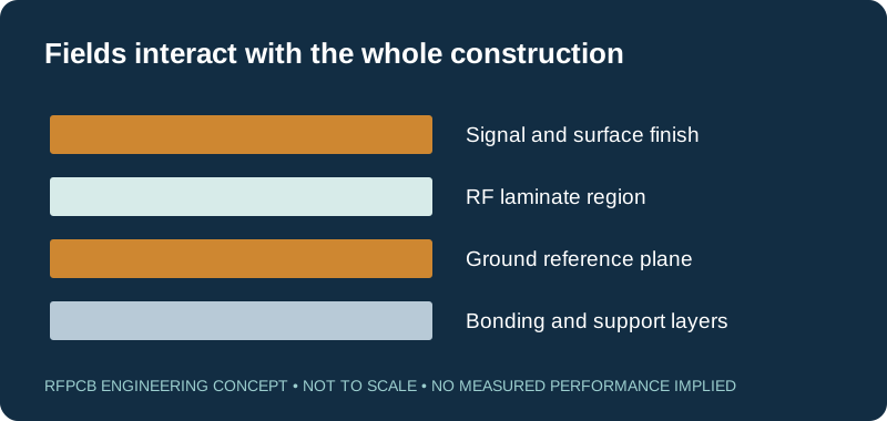
A multilayer construction needs more than a list of copper layers. State the dielectric product between each relevant pair, the pressed thickness and the reference plane for each controlled route. Fields can extend into bonding material, so a core-only model may omit a meaningful part of the structure.
Use the RF stackup library for discussion examples, then request a project-specific drawing. Examples are not stock constructions or approvals. Confirm compatible materials, lamination sequence and thickness tolerances before routing the final design.
Compare finished-board cost and change risk
Raw laminate pricing is only one component of the finished-board quotation. Panel utilization, process steps, setup, inspection and expected yield can alter the result. If a new material changes line widths, bonding or testing, the engineering cost belongs in the comparison too.
For an established product, compare retaining the RF material with a different support stackup against replacing the RF material itself. These alternatives can have different qualification burdens. The cost planning page and material-change break-even tool keep those assumptions separate from a supplier commitment.
Design an evidence-based qualification plan
Choose tests that answer the reason for the material decision. A line-loss concern calls for an appropriate RF structure and defined reference planes. A dimensional concern calls for a measurement plan on the relevant features. A thermal concern requires operating and assembly conditions, not only room-temperature inspection.
Use comparable samples and record the construction and lot information. If the alternative requires tuning or geometry changes, document them. Approval should identify the final manufacturing revision and acceptance results, not simply state that a trial board powered on or passed a continuity test.
Write a useful material selection brief
A short selection brief should state the application, band, loss and impedance needs, environmental conditions, mechanical constraints, quantities and schedule. Identify any mandatory manufacturer grade and whether alternatives are allowed. Include open questions so they can be resolved before a quotation is mistaken for a design approval.
For specific candidates, continue to the PTFE PCB guide, RO3003 page or RO4350B page. Those grade-level discussions are the next step after a family-level comparison.
Prepare a reviewable engineering request
Check only the requirements you have actually documented. This list records readiness; it does not inspect your files or certify a design. Missing information is useful: identify it explicitly so the engineering review can resolve it before a production release.
These inputs are processed in your browser and are not submitted by this tool. The downloaded summary is a plain-text planning record. Use the secure quote form to send files; request an NDA first if your project requires one.
Manufacturing context
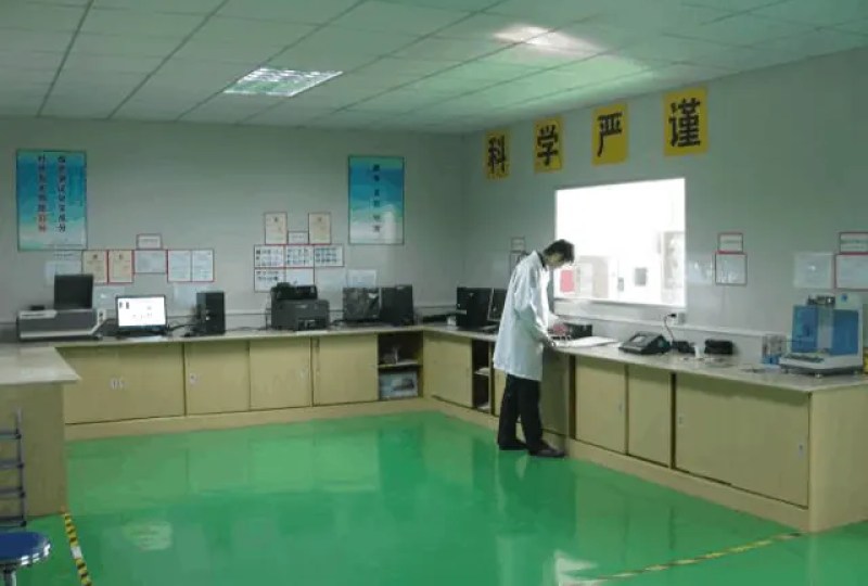
RFPCB and PCBSync share the manufacturing facility shown below. These process photographs illustrate the production environment; they are not evidence that a particular board, material grade or RF performance has been qualified. Request the documentation and inspection scope applicable to your project.


PTFE vs hydrocarbon laminate FAQs
Are all PTFE PCB materials unreinforced?
No. RF products can use different fillers or reinforcements. Check the exact manufacturer grade. The resin-family name does not determine the laminate structure, dielectric constant or mechanical behavior.
Is hydrocarbon laminate the same as standard FR-4?
No. A hydrocarbon/ceramic RF thermoset and a conventional glass-epoxy FR-4 product are different material systems. Similarities in some fabrication operations do not make their electrical properties or purchasing specifications interchangeable.
Does every PTFE board cost more?
There is no universal finished-board price rule. The exact material, construction, quantity, processing and acceptance scope determine the quotation. Compare like-for-like reviewed builds instead of applying a fixed family price multiplier.
Can these material families appear in one hybrid board?
Potentially, subject to an approved construction and compatible manufacturing process. Bonding, thickness, dimensional behavior and electrical models must be reviewed together. A generic hybrid sketch does not establish manufacturability.
Continue your engineering review
Turn a material-family choice into a buildable stackup
Send your candidate grades and circuit requirements. Request a proposed layer construction, processing review and quotation with a clear acceptance scope.
Sources and engineering scope
Manufacturer values apply to the identified grade, test method and construction. Engineering examples on this page are illustrative; they are not measured product results, inventory statements or certification claims. Rogers product names are trademarks of their owner. Keep the applicable datasheet revision with your approved manufacturing package.
Ready for a quotation?
Send your requirements for a material, stackup and manufacturing review. Price and schedule are confirmed for your project.