
RF material comparison · PTFE and thermoset
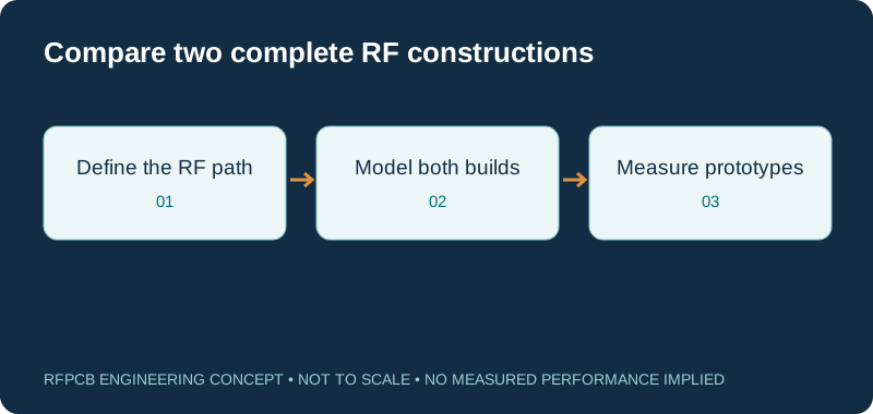
RO3003 vs RO4350B compares different material systems, not just two dielectric constants. Use the electrical requirements, manufacturing construction and qualification effort to decide which candidate deserves a prototype.
RO3003 is a ceramic-filled PTFE candidate for demanding low-loss RF paths. RO4350B is a reinforced hydrocarbon/ceramic thermoset candidate with a different fabrication route. Neither is a universal replacement for the other; compare the complete stackup, copper and finished-circuit evidence.
Reference properties and manufacturing implications
| Item | RO3003 | RO4350B |
|---|---|---|
| Material system | Ceramic-filled PTFE | Glass-reinforced hydrocarbon/ceramic thermoset |
| Typical process Dk | 3.00 ± 0.04 | 3.48 ± 0.05 |
| Typical Df at 10 GHz | 0.0010 | 0.0037 |
| Model selection | Obtain the applicable design model and document revision | Keep design and process characterization distinct |
| Manufacturing review | PTFE-compatible hole preparation, handling and bonding | Thermoset-compatible process and bonding plan |
| Finished-board selection | Loss, phase, construction and qualification together | Loss, cost, construction and qualification together |
Resonance sensitivity explorer
f₂ = f₁ × (L₁/L₂) × √(εeff₁/εeff₂). Hold geometry and coupling assumptions consistent. These are effective permittivities from a transmission-line model, not automatically the published bulk or process Dk. The calculation illustrates sensitivity rather than synthesizing a filter.
Start with the electrical problem you are solving
A material comparison becomes useful when it starts with a measurable constraint. That could be loss over a long feed route, phase consistency across channels, a resonator tolerance or a required operating-temperature range. “Higher frequency” alone is not a complete requirement because route length and circuit topology also determine sensitivity.
Write the operating band, representative path and acceptance target before requesting a material change. A short RF connection may need a different optimization from a distributed filter or antenna feed. The goal is a construction that meets the product requirement with an understood manufacturing process.
Why the material family matters to fabrication
Ceramic-filled PTFE and reinforced thermoset laminates require different process considerations. Hole preparation, surface treatment, dimensional compensation, material handling and bonding should be reviewed as a complete manufacturing route. A process that works for one family is not automatically a released process for another.
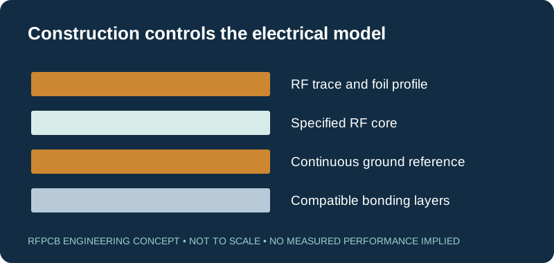
For a multilayer design, ask which dielectric regions use the selected RF material and which bonding products connect them. The electrical model must include the regions that carry significant fields. A stackup described only as “Rogers plus FR-4” omits details that matter to both manufacturing and circuit behavior.
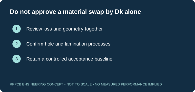
Do not mix process Dk, design Dk and effective permittivity
Keep each property tied to its method and intended use. Process-control Dk values are useful material references, while an electrical design needs the model appropriate to the geometry and construction. Effective permittivity is a property of the guided structure and is not automatically equal to either published value.
The Rogers online material table and a downloaded datasheet can reflect different revisions or conventions. Record the specific source used for a model rather than silently replacing one number with another. For a critical circuit, correlation with an agreed coupon or prototype is more useful than an unexplained spreadsheet constant.
Evaluate loss over the path you actually build
A lower dielectric-loss reference can make a material attractive, but the benefit at the connector depends on the rest of the design. Include conductor roughness, trace dimensions, finish, bends, vias and launches. A material change that also requires much narrower lines can alter the conductor contribution and the tolerance sensitivity.
Use the insertion-loss planning tool to organize assumptions, then choose a simulation and measurement method appropriate to the circuit. A simple line estimate cannot establish the performance of a complex transition, coupled structure or assembled RF module.
Understand resonance and phase sensitivity
For a fixed idealized path, increasing effective permittivity lowers its resonance and increases its electrical length at a given frequency. The sensitivity explorer makes this relationship visible without pretending to synthesize a complete filter. Change one input at a time and keep a note of which parameter came from a model and which was an assumption.
Coupling, end effects and connector loading can invalidate a simple scaling estimate. For resonators or phased feeds, review the entire relevant geometry. If the project requires tuning, define the allowed tuning features and how their final dimensions will be controlled in production.
Consider a hybrid construction before a full redesign
Sometimes the economical option is to retain the validated RF layer while changing the support construction. Other projects need a different RF dielectric to meet the loss budget. These are distinct engineering changes and should be quoted separately so that their costs and risks remain visible.
The hybrid stackup page explains the manufacturing information needed for that discussion. Preserve a continuous reference plane beside sensitive RF routes and identify the bonding layers. Confirm thickness balance, press sequence and dimensional requirements before releasing an updated mechanical design.
Build a cost comparison that includes qualification
Compare delivered boards with the same quantity, finish and test scope. Include setup, material allocation and special processing, then add the engineering work required to validate the alternative. A nominally cheaper laminate is not automatically a cheaper approved product when another layout iteration or RF test campaign is needed.
Use the alternative-material break-even tool to include the qualification budget. Ask for prototype and repeat-production quantities separately. This keeps the decision focused on the actual purchasing plan instead of an unsupported percentage saving.
Specify what the supplier must report
Material traceability, finished thickness, critical dimensions, impedance and RF measurements answer different questions. Identify which evidence is required for this particular build. A continuity test does not establish insertion loss, and a TDR coupon does not establish the center frequency of an assembled filter.
For RF acceptance, define the test article, fixture, frequency sweep, reference planes and limits. If the manufacturing supplier is providing bare boards only, state who will assemble and measure the prototype. A clear division of responsibilities prevents important validation work from being assumed rather than performed.
Release the selected construction as a controlled package
After comparison, freeze one consistent set of manufacturing inputs: fabrication data, drill files, stackup, approved material designations and test requirements. Identify allowed substitutions explicitly. Keep the baseline prototype results with the same revision so future changes can be assessed against meaningful evidence.
Use the dedicated RO3003 PCB page for material-specific planning, or the RO4350B PCB page for the thermoset option. The choice should remain understandable to a buyer who did not participate in the original RF design review.
Prepare a reviewable engineering request
Check only the requirements you have actually documented. This list records readiness; it does not inspect your files or certify a design. Missing information is useful: identify it explicitly so the engineering review can resolve it before a production release.
These inputs are processed in your browser and are not submitted by this tool. The downloaded summary is a plain-text planning record. Use the secure quote form to send files; request an NDA first if your project requires one.
Manufacturing context
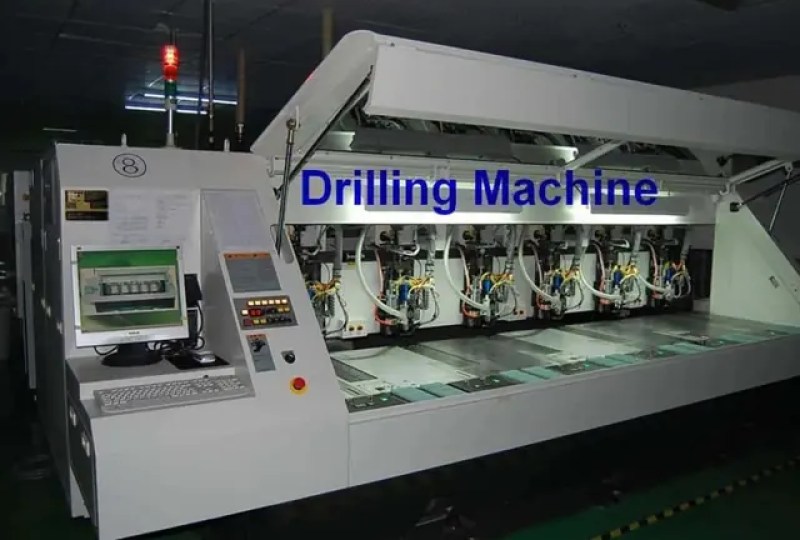
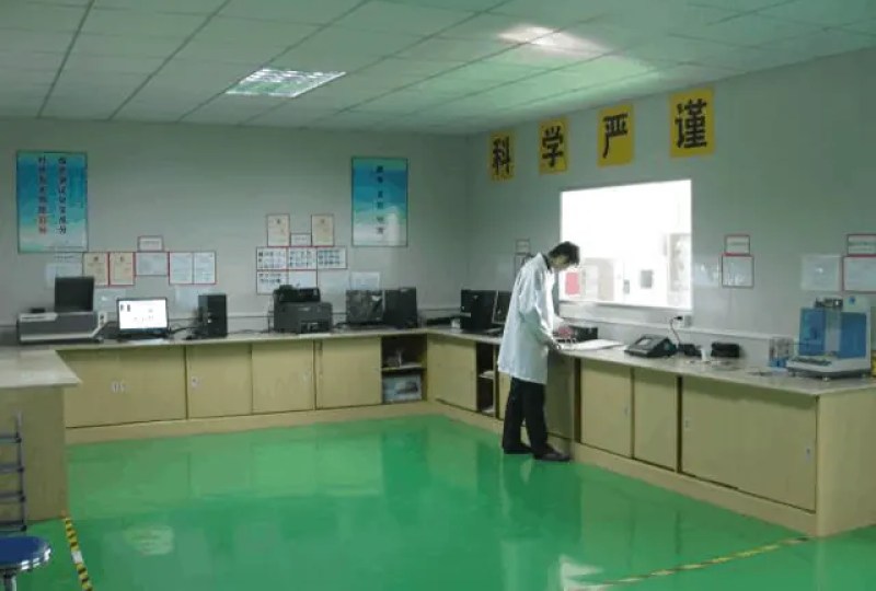
RFPCB and PCBSync share the manufacturing facility shown below. These process photographs illustrate the production environment; they are not evidence that a particular board, material grade or RF performance has been qualified. Request the documentation and inspection scope applicable to your project.

RO3003 vs RO4350B FAQs
Is RO3003 only for millimeter-wave boards?
No. A material can be considered wherever its electrical and manufacturing properties fit the requirement. A frequency label alone does not determine suitability. Route length, losses, geometry and environmental conditions are also part of the selection.
Is RO4350B unsuitable at high frequencies?
There is no universal cutoff that makes every RO4350B circuit unsuitable. Evaluate the actual path and performance requirements. A design with a short route and generous loss budget differs from a long, tightly controlled distributed network.
Can the resonance tool calculate my final filter dimensions?
No. It scales an idealized electrical length using effective permittivity. Coupling, dispersion, end corrections, discontinuities and assembly effects require a more complete model and prototype validation.
What should I send for a comparison quotation?
Send one baseline fabrication package, the allowed alternative, quantities and test scope. Identify which constraints must remain fixed and which may change. Ask for the proposed stackup and any geometry changes alongside the price.
Continue your engineering review
Request a construction-specific material comparison
Share your loss budget, sensitive geometry and approved baseline. We can review the proposed manufacturing constructions and identify the questions to resolve before qualification.
Sources and engineering scope
Manufacturer values apply to the identified grade, test method and construction. Engineering examples on this page are illustrative; they are not measured product results, inventory statements or certification claims. Rogers product names are trademarks of their owner. Keep the applicable datasheet revision with your approved manufacturing package.
Ready for a quotation?
Send your requirements for a material, stackup and manufacturing review. Price and schedule are confirmed for your project.