

Manufacturing capability · RF and microvia integration
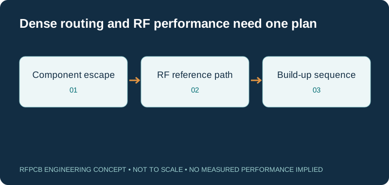
HDI RF PCB manufacturing combines dense interconnection with controlled RF paths. Review the material, microvia structure and build-up sequence together so that component escape routing does not compromise the signal reference or manufacturing plan.
An HDI RF PCB uses dense interconnect features such as microvias alongside RF circuitry. A generic HDI capability does not automatically qualify every Rogers or PTFE construction. Submit the exact layer pairs, dielectrics and acceptance requirements for a construction-specific review.
HDI RF construction review matrix
| Feature | What to provide | What engineering must resolve |
|---|---|---|
| Blind microvia | Start/end layer, depth, opening and landing geometry | Material compatibility, taper, registration and fill |
| Stacked or staggered vias | Layer-pair drawing and intended sequence | Lamination operations and reliability requirements |
| RF layer transition | Signal via, grounds, antipads and reference planes | Return-path continuity and RF model |
| Hybrid dielectric build | Exact cores and bonding regions | Press plan, dimensions and electrical model |
| Fine-pitch component escape | Package pitch, pad and routing rules | Capture-pad and assembly process compatibility |
| Acceptance evidence | Inspection, microsections and test requirements | Sample scope, methods and agreed limits |
Microvia geometry checker
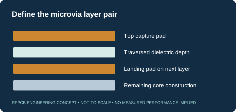
Aspect ratio = microvia depth / nominal opening diameter. Use the traversed dielectric depth, not total board thickness. Laser taper, landing diameter, capture pad, material and copper fill require separate review. This tool does not assign a universal pass/fail limit.
When HDI belongs in an RF board
Fine-pitch components, dense digital support circuitry and compact RF modules can create routing needs that ordinary through-hole interconnection cannot efficiently satisfy. HDI features may help with escape routing and layer access, but the reason for each feature should remain clear in the design brief.
Adding microvias is not automatically an RF improvement. A transition still needs an intentional return path and an appropriate electromagnetic model. Evaluate the interconnection in its surrounding geometry rather than assuming a smaller hole solves every mismatch or coupling problem.
Distinguish factory capability from an approved construction
The shared PCBSync factory capability material describes HDI, blind and buried via work and sequential lamination. Those general capabilities support an engineering discussion, but they do not establish that every combination of RF laminate, dielectric depth, pad size and stacked structure is approved for your project.
This page therefore does not publish a universal minimum microvia or guaranteed layer count for all RF materials. Send the exact stackup and feature drawing. The manufacturing response should identify a proposed process, relevant constraints and any evidence required before a new construction is released.
Define microvia depth and diameter precisely
The aspect-ratio tool divides the traversed dielectric depth by the nominal opening diameter. Enter both in micrometers. Do not use total board thickness for a microvia that connects only adjacent build-up layers. If the via is tapered, the opening, bottom and landing geometry are different dimensions and should be identified in the drawing.
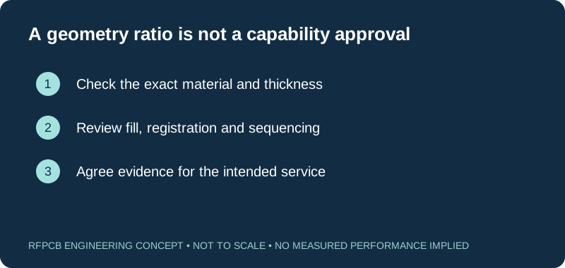
A favorable ratio does not prove manufacturability. Material response, laser process, capture pad, registration, copper fill and inspection all matter. The tool intentionally reports geometry without declaring a universal pass or fail. Obtain the applicable limits from the construction review.
Choose stacked or staggered structures deliberately
A stacked arrangement and a staggered arrangement can have different process and reliability implications. Show the intended connection layer by layer, including whether vias are filled and capped. Avoid leaving the manufacturing sequence to inference from separate drill files or a schematic net name.
Ask engineering to confirm the number and order of build-up operations for the proposed design. If an alternative via arrangement is suggested, review its impact on routing area, reference continuity and component placement. Keep the accepted structure in the released stackup and fabrication notes.
Keep RF transitions tied to their reference planes
A signal changing layers needs a defined path for its return current. Ground connections, plane openings, antipads and nearby metal influence the transition. A nominally controlled line on each side does not establish the performance of the connection between them.
For important transitions, supply the relevant geometry and reference planes to the RF model. Use the controlled-impedance page to define routed-line requirements, then treat via and connector transitions as separate structures where necessary. Manufacturing DFM and electrical validation should inform each other without being confused.
Review RF and digital regions in a hybrid build
A compact module may place RF functions beside dense digital or power circuitry. Identify which dielectric regions must use the selected RF laminate and which may use another approved system. The fields around sensitive routes and transitions determine where the material properties matter.
The hybrid stackup guide helps organize this discussion. Include bonding materials, pressed thicknesses and copper balance. A construction that routes conveniently in CAD still needs a compatible lamination plan and a clear tolerance budget for its electrical and mechanical interfaces.
Connect via-in-pad decisions to assembly requirements
Where vias are placed in component pads, the fabrication and assembly teams need a consistent definition of fill, cap and surface condition. A component escape solution that ignores soldering behavior can introduce problems after the bare board has passed inspection. Provide the package and assembly requirements early.
Use the RF assembly guide when requesting populated boards. RF grounding pads and matching networks can be electrically sensitive, so proposed assembly-driven changes should also be reviewed by the circuit designer. Preserve the agreed details in the final fabrication and assembly drawings.
Specify inspection and reliability evidence
Agree which structures need dimensional inspection, microsection evidence, continuity testing or other qualification. Identify the construction and service conditions to which the requirements apply. A report on a generic coupon or different stackup does not automatically establish the behavior of the proposed build.
For a new or demanding structure, distinguish development qualification from routine production acceptance. Ask what evidence is available and what additional work must be planned. The quotation should state the sample and reporting scope instead of implying that every advanced reliability test is automatically included.
Prepare an HDI RF quotation package
Include the layer stackup, via layer-pair drawing, dielectric depths, pad geometry, copper requirements, board dimensions and quantities. Mark controlled RF routes, critical transitions and any special assembly requirements. Identify the design revision and whether alternatives such as staggered vias may be proposed.
Use the RF DFM checklist to record open decisions. Cost can depend on build-up operations, filling, material allocation and inspection, so request a construction-specific quotation. A single hole diameter or layer count cannot describe the manufacturing job accurately.
Prepare a reviewable engineering request
Check only the requirements you have actually documented. This list records readiness; it does not inspect your files or certify a design. Missing information is useful: identify it explicitly so the engineering review can resolve it before a production release.
These inputs are processed in your browser and are not submitted by this tool. The downloaded summary is a plain-text planning record. Use the secure quote form to send files; request an NDA first if your project requires one.
Manufacturing context
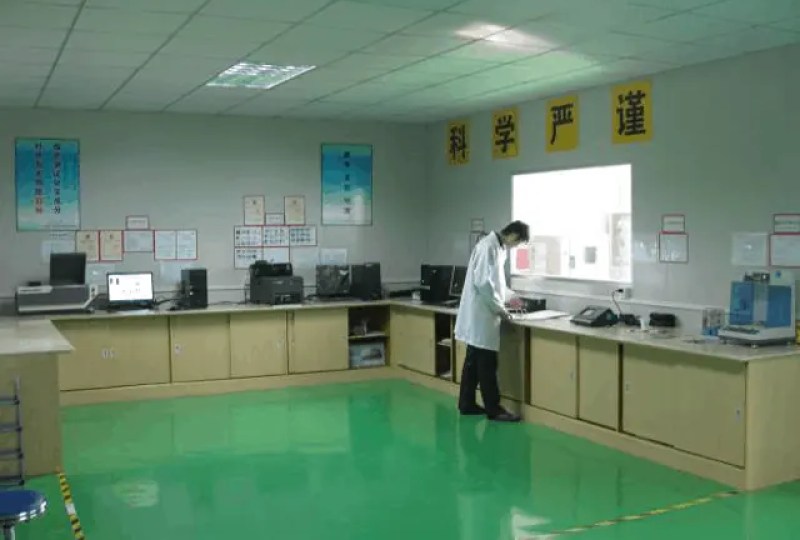
RFPCB and PCBSync share the manufacturing facility shown below. These process photographs illustrate the production environment; they are not evidence that a particular board, material grade or RF performance has been qualified. Request the documentation and inspection scope applicable to your project.


HDI RF PCB FAQs
Can every HDI process be used on every RF laminate?
No. The material, thickness, via geometry and lamination sequence must be reviewed together. General factory HDI capability is not a blanket approval for any PTFE, thermoset or hybrid RF construction.
Does a low microvia aspect ratio guarantee reliability?
No. The ratio describes one geometric relationship. Fill, interfaces, material, process controls, assembly and service conditions also matter. Agree the applicable construction review and qualification evidence before production.
Are microvias always electrically better than through vias?
Not automatically. The complete transition and return path determine electrical behavior. A smaller structure may offer useful design options, but it still needs modeling and validation in the surrounding stackup and circuit.
What should I send before finishing the layout?
Send a proposed stackup, package escape requirements, via layer pairs, target geometries and RF constraints. Early review can identify construction issues before the layout depends on an unapproved feature. Final acceptance still requires the complete release package.
Continue your engineering review
Review the HDI construction before routing is frozen
Share the stackup, microvia layer pairs and RF transition requirements. Request a manufacturing proposal with explicit process assumptions, inspection scope and open engineering questions.
Sources and engineering scope
- PCBSync shared-factory rigid PCB capabilities
- Rogers RO4000 manufacturer datasheet
- Rogers RO3000 family properties and documents
Manufacturer values apply to the identified grade, test method and construction. Engineering examples on this page are illustrative; they are not measured product results, inventory statements or certification claims. Rogers product names are trademarks of their owner. Keep the applicable datasheet revision with your approved manufacturing package.
Ready for a quotation?
Send your requirements for a material, stackup and manufacturing review. Price and schedule are confirmed for your project.