
RF MANUFACTURING / QUOTATION TO RELEASE
Useful RF PCB fabrication notes identify the exact construction, the features that must stay fixed, the evidence required for acceptance and the questions that remain open. Each note should point to a drawing, table or file revision that the fabricator can inspect. A quotation package may contain documented assumptions; a manufacturing release needs those assumptions resolved or explicitly accepted by the responsible design owner.
This guide works through an illustrative note set and change record. It complements a general DFM checklist by showing how to turn phrases such as “50 ohms,” “gold finish” and “equivalent material allowed” into reviewable instructions. The sample identifiers are fictional and carry no production approval. Use the RF PCB manufacturing capabilities overview to identify which parts of your construction need a specific engineering discussion.
1. Start with a package identity and a release state
Put the board part number, drawing revision, date, units and intended purpose on the fabrication drawing. Include a manifest naming the copper, mask, legend, profile, drill, stackup and test documents. If several quantities are being priced, keep them in the commercial request so they cannot be mistaken for different board definitions.
Ucamco’s Gerber Job Format Specification, revision 2020.08, section 2.1, separates technical board characteristics from commercial conditions. It also makes clear that an absent characteristic does not acquire a default value from the format. A job file can carry useful fabrication information, but check which fields your exporter supplies and which the receiving workflow reads.
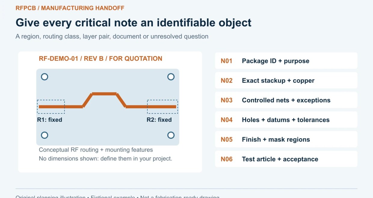
Our fictional package is RF-DEMO-01, revision B, FOR QUOTATION. Its manifest lists a fabrication drawing, layer files, drill data and stackup proposal S2. Issue Q-03 remains open: the supplier must propose a manufacturable width for one controlled routing class. Calling the whole package “final” would hide that unresolved electrical decision.
A practical status vocabulary is specified, supplier proposal required and approved for this revision. Record an owner for every unresolved item. These are suggested project controls, not standardized file-format attributes or automatic approvals created by the website.
2. Write a material note that identifies the construction
Example N02: “Build to stackup S2 after approval. Identify manufacturer, exact laminate and bonding grades, nominal dielectric thicknesses, proposed pressed thicknesses, copper foil and finished copper requirements by layer. Submit substitutions as separate proposals; do not incorporate them without recorded approval.”
A brand name alone is insufficient for purchasing or process planning. Distinguish a core thickness from the finished board thickness, and base foil from finished plated copper. Where electrical modeling depends on a dielectric value, retain its source, method, frequency and revision with the stackup record. Do not use an unspecified generic Dk as an acceptance test for incoming material.
Process guidance is construction-specific. Rogers’ RO4000 LoPro processing guide, publication 92-418, 2020 revision, directs multilayer bonding decisions to the selected adhesive system’s guidance. This is a reason to name the bond material, not a reason to copy a generic press cycle into every RF drawing.
AGC’s RF-35TC general processing guide also discusses RF-35A2 and TSM-DS3 and states that suitable parameters depend on processing equipment. A familiar filename does not make every section applicable to every grade. Attach the relevant source and ask the fabricator to confirm its qualified route rather than prescribing an unreviewed machine recipe.
3. Give the impedance note a controlled scope
Example N03: “Controlled routing class RF_A is single-ended microstrip on L1 referenced to L2. Nominal target is 50 Ω. Proposed tolerance, finished geometry, mask condition and coupon method require approval before fabrication. Regions R1 and R2 contain electrically fixed launch geometry; changes require design-owner review.”
This is an RFQ instruction, not a complete release note. Replace the open fields with agreed values before manufacture. Include the actual net list or routing-class mapping so the instruction does not accidentally apply to every line on the board. For coplanar or differential structures, add the relevant gap or pair-spacing definition and use the matching model.
The 50-ohm trace tolerance worksheet shows how width, dielectric height and permittivity interact. Its assumed values must not be copied into a fabrication drawing as factory limits. Save your project’s model and sensitivity review with the approved stackup, including the definition of finished width.
Separate permission to propose a width adjustment from permission to implement one. A line-width change can affect a matching network, coupler or resonator even if it improves the nominal impedance of a straight trace. Mark the protected geometry and require an explicit disposition for it.
4. Tie holes, surfaces and dimensions to named features
Example N04: “Use hole schedule H1 and the matching drill files. Identify plated and nonplated features, finished hole dimensions and tolerances, slots, layer spans and any fill or cap requirements. Resolve differences between the schedule and machine-readable data before processing.”
Specify datum references for connector mounting, cavities and critical outline features. A back-drilled feature needs a reviewed layer relationship and residual-stub requirement, not just the word “backdrill.” Avoid adding a tight global tolerance when only a few RF-sensitive features require it; identify the features and their functional reason.
Example N05: “Surface finish and solder-mask coverage shall match drawing regions F1 and M1 after approval. Confirm the selected finish stack and inspection requirements. No mask, legend or panel breakaway feature may enter the marked RF keepout without engineering approval.”
“Gold” leaves the finish process unclear. Likewise, “no mask on RF” does not define a boundary that CAM can reliably apply. Give region names, layer identities and actual geometry. Check that the mask artwork agrees with the note. A dimensioned PDF is valuable context, but it should not quietly contradict the released copper or mask data.
5. Replace ambiguous notes with evidence-linked instructions
| Ambiguous phrase | Useful replacement | Evidence to close it |
|---|---|---|
| Equivalent material OK | List a candidate separately and identify all construction changes. | Approved grade, foil, bonding and electrical-model review. |
| All RF traces 50 Ω | Name the controlled class, layers, references and fixed regions. | Agreed geometry, tolerance and coupon plan. |
| Gold, standard mask | Identify the finish process and map mask coverage to regions. | Consistent finish note and mask artwork. |
| RF tested | State the test article, method, band, limits and report. | Accepted test plan with responsibilities and fixture scope. |
Use the interactive preparation tool: work through the RF PCB DFM checklist. In its project-notes field, record each open note ID, its owner and the required response. Copy or download the summary and attach it to the RFQ. Checking a box records your assessment; it does not inspect files or release the board.
6. Work one change from quotation to release
In the fictional revision B package, Q-03 asks for a proposed width for RF_A while R1 and R2 stay fixed. The supplier replies with stackup S3, a geometry proposal and a description of the affected routing. The design owner must evaluate the complete proposal; “S3 accepted” is ambiguous if the copper files still reflect S2.
- Record the proposal: identify the affected layer, routing class, construction inputs and excluded fixed regions. Keep the original RFQ files unchanged as a historical record.
- Evaluate the electrical effect: update the relevant model and check transitions into the protected regions. Record what was calculated, simulated or measured and what remains unverified.
- Resolve the files: issue a coherent revision C with the accepted geometry, stackup S3, revised note N03 and matching output files. Review the regenerated package instead of relying on an email attachment alone.
- Close Q-03: record approver, date, decision and the exact package identity. The supplier acknowledges that package before the manufacturing release proceeds.

A material substitution follows the same control path. An acceptable price or delivery proposal does not establish electrical equivalence. If an alternative needs validation, keep it visibly conditional and identify who owns that work. Do not silently convert “quote this option” into “build this option.”
7. State what the acceptance report must prove
Example N06: “Use the approved inspection and test plan T1. Identify the test article, method, conditions, acceptance limits, coverage and report fields for each requirement. Confirm any special fixture or RF measurement scope in the quotation.”
Continuity and isolation checks, an impedance coupon and a frequency-domain RF measurement answer different questions. A coupon result does not establish the return loss of an assembled connector launch. If that behavior is contractual, specify the operating band, measurement reference planes, fixture treatment, limits and responsibility for supplying the assembled test article.

Request applicable quality and test documentation against the actual build. If a customer requires a particular standard, class or certification, identify its edition and scope and obtain confirmation. Do not substitute a website capability table for an order-specific acceptance agreement.
8. Run a final package reconciliation
Open the exported fabrication data independently of the PCB editor and compare it with the drawing. Check the layer sequence, units, origin, board profile, hole map, mask exclusions and controlled-net definitions. Confirm that the manifest names the files actually present and that obsolete alternatives have been removed from the outgoing package.
Review every “TBD,” “standard,” “equivalent” and “as discussed” phrase. Either replace it with the agreed definition or identify the remaining decision and release restriction. Archive the final package and approval record together. A later repeat order should identify that released revision rather than an old quote subject line.
Send your fabrication package for DFM review
Provide Gerber or indicate ODB++ availability for format confirmation, drill data, a fabrication drawing, the package revision and the requested inspection scope. Include the stackup, critical RF regions, proposed test plan and open-issue record. State whether the request is for quotation, prototype review or manufacture so the response can address the right decision.
Send your fabrication package for DFM review
Engineering note checked 10 October 2026. The sample notes and figures are original planning examples, not fabrication-ready instructions. The AGC guide is accessed as an undated document; the Rogers publication and Ucamco specification revisions are identified above. Confirm applicable current revisions with your design and manufacturing teams.
Put this into production
Request a material, stackup and manufacturing review for your RF PCB project.