

What Is a Mixed Dk Stackup?
A mixed Dk stackup is a PCB construction that uses two or more laminates with different dielectric constants (Dk) in a single board. RF-critical layers get a low-loss, tightly controlled material such as RO4350B (Dk 3.48 ± 0.05) or RO3003 (Dk 3.00 ± 0.04), while power, ground, and digital routing layers use standard FR-4 (Dk ≈ 4.2–4.5). The result is a board that meets RF performance targets at a fraction of the cost of an all-PTFE build—typically 30–50 % less, depending on layer count and material split.
This approach is the backbone of most modern radar front-ends, 5G massive-MIMO feed networks, and satcom LNBs. If you are evaluating whether to mix Rogers and FR-4 in one board, the answer is almost always yes—but the details of how you pair, bond, and control impedance across the material boundary determine whether the board actually works.
Why Mix Dielectrics Instead of Using One Material?
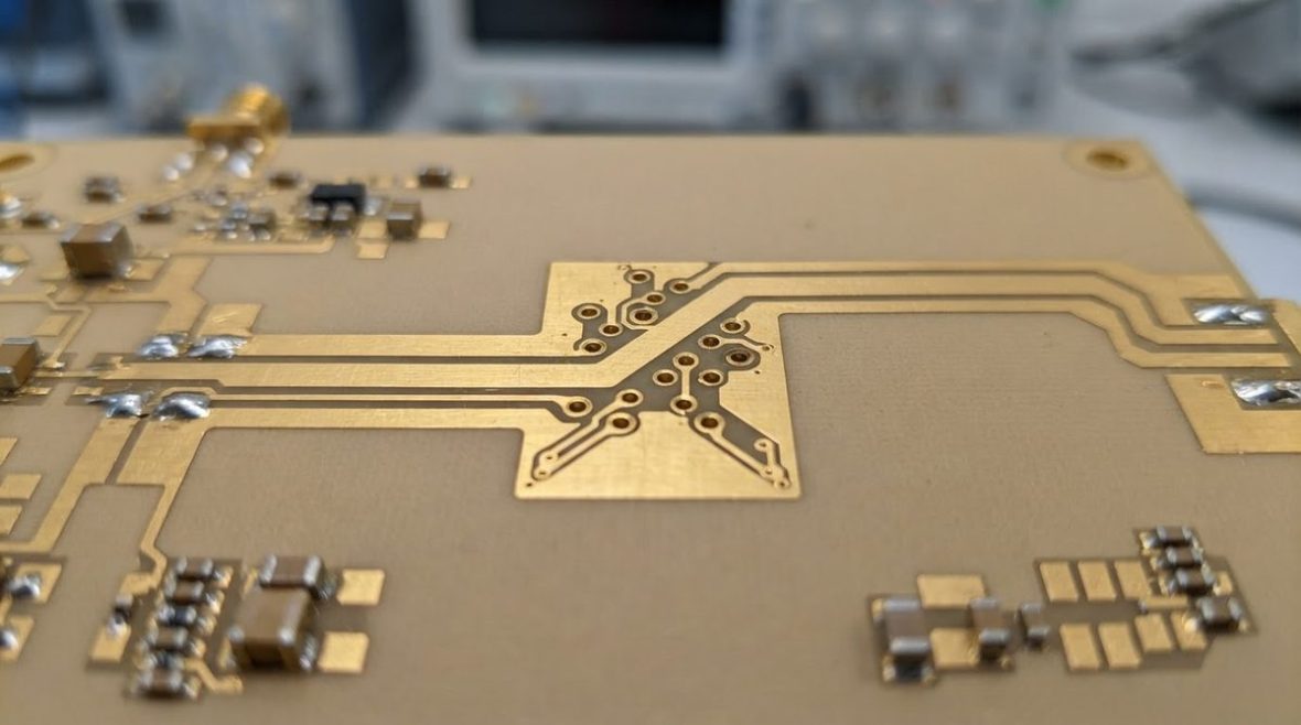
Three forces push designers toward a mixed Dk stackup:
- Cost. High-frequency laminates cost 5–20× more per panel than FR-4. Limiting them to two or four layers instead of twelve saves material and press cycles.
- Mechanical compatibility. Pure PTFE boards are soft, difficult to drill, and prone to pad lift. An FR-4 core in the center adds rigidity and improves via reliability.
- Supply chain. FR-4 is available from dozens of qualified sources in every thickness. Specialty laminates have longer lead times and fewer alternatives.
The trade-off is complexity: two materials mean two sets of Dk/Df values, two CTE profiles, and a bonding interface that must survive reflow without delamination. Every one of those issues is manageable—but only if the stackup is designed for it from the start.
Choosing the Right Material Pairing
The most common mixed Dk pairings in production today fall into three families:
| RF Laminate | Dk (10 GHz) | Df (10 GHz) | Typical Partner | Common Application |
|---|---|---|---|---|
| RO4350B | 3.48 | 0.0037 | FR-4 (Tg 170 °C) | Sub-6 GHz 5G, Wi-Fi 6E |
| RO4835 | 3.48 | 0.0040 | FR-4 (high-Tg) | Automotive V2X, C-band |
| RO3003 | 3.00 | 0.0013 | RO4350B or FR-4 | 77 GHz automotive radar |
| CLTE-XT | 2.94 | 0.0012 | FR-4 or polyimide | Ku/Ka-band satcom |
| Megtron 6 (R-5775) | 3.40 | 0.0020 | Standard Megtron 4 | High-speed digital + RF hybrid |
When selecting a pair, match these parameters in order of priority: (1) Z-axis CTE—keep both materials within 10 ppm/°C of each other or use a bondply that bridges the gap; (2) Tg and Td—the lower-rated material sets the reflow ceiling; (3) copper-peel strength—mixed interfaces are only as reliable as the weaker bond. For a deeper comparison of laminate families, the high-frequency PCB materials guide covers Rogers, Taconic, Isola, and Panasonic grades side by side.
Planning the Layer Pairing with a Mixed Technology Planner
The first concrete design step is deciding which layers get which material. A typical 8-layer mixed Dk stackup might look like this:
- L1 (RF signal): RO4350B, 6.6 mil (0.168 mm) core
- L2 (ground): copper on same RO4350B core
- L3–L6 (power/digital): FR-4 cores + prepreg
- L7 (ground): copper on RO4350B core
- L8 (RF signal): RO4350B, 6.6 mil core
This symmetric arrangement keeps the RF laminates on the outer pairs and FR-4 in the middle, which simplifies press layup and avoids warpage from CTE mismatch. Enter your own layer count, material choices, and target impedances into the planner below to see whether your proposed split is manufacturable.
If the planner flags a CTE mismatch warning, the usual fix is to swap the FR-4 prepreg at the material boundary for a hybrid-compatible bondply such as RO4450F (Dk 3.52, CTE-z 35 ppm/°C), which is specifically formulated to bond thermoset laminates to FR-4. This adds roughly $2–4 per panel but eliminates the dominant delamination risk. Fabricators experienced with hybrid stackup PCB builds will already stock these bondplies.
Managing Dk Drift Across Temperature and Frequency
Every dielectric constant printed on a datasheet is measured at a single frequency and temperature—typically 10 GHz and 23 °C. In a mixed Dk stackup, the two materials drift at different rates, which means the impedance delta between your RF layer and your digital layer changes with operating conditions.
How Much Does Dk Actually Drift?
RO4350B has a thermal Dk coefficient of roughly +50 ppm/°C; standard FR-4 can exceed +200 ppm/°C. Over a 60 °C temperature swing (from room temperature to a typical enclosure interior), that is:
- RO4350B: Dk shifts from 3.48 to ≈ 3.49 (+0.3 %)
- FR-4: Dk shifts from 4.30 to ≈ 4.35 (+1.2 %)
A 1.2 % Dk change on an FR-4 digital layer rarely matters. But if you accidentally route a 2.4 GHz filter matching network on the FR-4 layer because “it fit better,” that same drift translates to roughly 0.6 % impedance shift—enough to move a narrowband filter’s center frequency by several MHz. Understanding why datasheets show different Dk values for the same material helps you pick the right number for your simulation.
Use the estimator below to see how Dk drift in each material affects impedance over your expected temperature range.
If the estimator shows more than ±1 Ω drift on a 50 Ω line, consider tightening the Dk tolerance specification on your RF laminate (Rogers offers “design Dk” vs. “process Dk” grades) or moving the sensitive trace to the more stable material. For lines that must stay on FR-4, widen the trace slightly to reduce the impedance sensitivity to Dk changes—a wider microstrip’s impedance depends more on geometry and less on dielectric constant.
Impedance Control at the Material Boundary
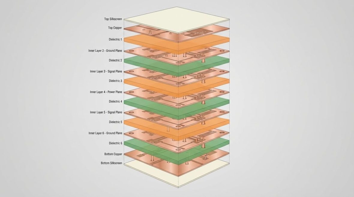
The trickiest spot in any mixed Dk stackup is where a via transitions a signal from a low-Dk layer to a high-Dk layer. The characteristic impedance of the via barrel changes as it passes through different dielectrics, creating a localized impedance discontinuity. At frequencies below about 6 GHz this is usually negligible; above 10 GHz it can add 1–3 dB of return loss at the transition.
Mitigation Techniques
- Back-drilling. Remove the unused via stub that extends past the target layer. A stub sitting in FR-4 (Dk 4.3) resonates at a lower frequency than one in RO4350B (Dk 3.48), so mixed stackups make stub control even more critical. Details on depth tolerances are covered in the back-drilled stackup guide.
- Via antipads tuned per layer. Use a larger antipad in the higher-Dk layers to compensate for the increased capacitance. A 25 mil (0.64 mm) antipad in FR-4 layers vs. 20 mil (0.51 mm) in Rogers layers is a common starting point for a 10 mil drill.
- Transition pads. Add a short coplanar-waveguide launch pad on the target layer to re-establish the impedance before the microstrip continues. This costs board area but buys 5–8 dB of return-loss improvement above 20 GHz.
For pre-calculated trace widths on each material, the impedance reference tables list 50 Ω and 100 Ω differential geometries across common core thicknesses.
Fabrication Notes for Mixed Dk Boards
Lamination Cycle
FR-4 prepreg cures at 175–185 °C under 250–400 psi. Most thermoset RF laminates (RO4000 series, Megtron 6) tolerate these conditions, but PTFE-based materials (RO3003, RT/duroid) require lower pressure (50–100 psi) and sometimes a separate press cycle. Confirm your fabricator’s press capability before finalizing the material pair. Rogers’ RO4350B product page publishes recommended lamination profiles that most shops follow.
Drilling
PTFE laminates smear more than FR-4 during drilling. Mixed builds may need a two-step drill program: standard parameters for the FR-4 portion and reduced chip load for the PTFE layers. Laser-drilled microvias in the RF layers avoid this issue entirely but add cost.
Registration
Different materials shrink at different rates during lamination. Expect ±2 mil (0.05 mm) additional registration tolerance on a mixed Dk stackup compared to an all-FR-4 build. Account for this in annular-ring calculations and pad-to-trace clearances.
Common Mistakes to Avoid
- Routing RF traces on FR-4 “just for a short run.” Even 5 mm of FR-4 microstrip at 28 GHz adds measurable insertion loss and phase error. Keep every millimeter of the RF path on the intended laminate.
- Ignoring bondply Dk. The prepreg or bondply between dissimilar cores has its own Dk, which affects stripline impedance on the adjacent layer. Simulate with the actual bondply Dk, not the core Dk.
- Symmetric stackup violations. Placing Rogers only on the top and FR-4 everywhere else causes bow and twist that can exceed the IPC-6012 Class 3 limit of 0.75 %. Mirror the material placement around the board center.
- Specifying a single Dk for impedance calculations. Each layer must use the Dk of its own dielectric at the design frequency, not an average.
Design Checklist
- Identify which layers carry RF signals and assign the low-loss laminate to those layers only.
- Choose a bondply compatible with both materials (matched CTE-z, compatible cure profile).
- Build a symmetric stackup to control warpage.
- Run impedance simulations per layer, using each layer’s actual Dk at the operating frequency.
- Specify back-drill or blind vias for any signal crossing the material boundary above 6 GHz.
- Call out the material on each layer in the fabrication drawing—do not rely on a single “material” note.
- Verify Dk drift over your operating temperature range and confirm the impedance stays within budget.
Frequently Asked Questions
Can I use more than two different Dk materials in one stackup?
Yes. Three-material builds (e.g., RO3003 on outer RF layers, RO4350B on inner stripline layers, FR-4 for power/ground) are common in 77 GHz radar modules. Each additional material adds a press cycle and a bonding interface, so cost and lead time increase accordingly.
Does a mixed Dk stackup affect controlled-impedance yield?
It can. The tighter the Dk tolerance of the RF laminate (±0.05 vs. ±0.15 for FR-4), the better the impedance yield on those layers. Expect ±5 % impedance on Rogers layers and ±8–10 % on FR-4 layers within the same board.
Is a mixed Dk stackup the same as a hybrid stackup?
In practice, the terms are used interchangeably. “Mixed Dk stackup” emphasizes the dielectric-constant difference; “hybrid stackup” is the broader fabrication term that also covers mixed copper weights or mixed flex-rigid constructions.
What is the maximum frequency where FR-4 layers are still acceptable for digital routing?
Standard FR-4 (Df ≈ 0.020 at 10 GHz) works for digital signals up to roughly 5–8 Gbps depending on trace length. Above that, consider mid-loss laminates like Megtron 4 (Df ≈ 0.005) for the digital layers while keeping the RF layers on ultra-low-loss material.
Do I need to specify the mixed Dk stackup in my Gerber files?
Gerbers carry no material information. Document the stackup in a separate fabrication drawing or IPC-2581 file that calls out the material, thickness, and Dk for every dielectric layer. This is the single most important deliverable for a mixed Dk build.
Ready for a quotation?
Send your requirements for a material, stackup and manufacturing review. Price and schedule are confirmed for your project.