

What Is a Back Drill Stackup?
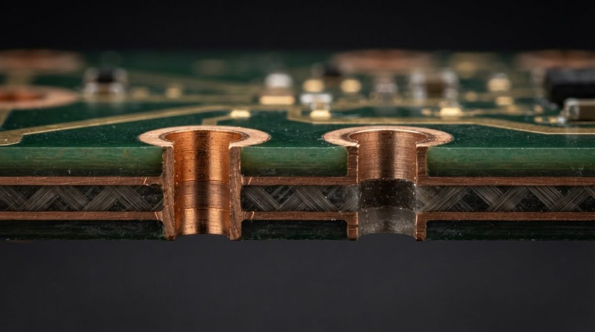
A back drill stackup is a multilayer PCB layer arrangement specifically designed so that unused via barrel sections—stubs—can be removed by controlled-depth counter-drilling from the opposite side of the board. The stackup defines where each signal transitions between layers and, therefore, how deep the back drill must reach and how much stub remains. Getting this right is the difference between a clean 28 GHz channel and one with a 15 dB resonant notch in the passband.
Back drilling matters once via stubs approach a quarter-wavelength at your operating frequency. For a stub in FR-4 (effective Dk ≈ 4.0), the quarter-wave resonance frequency is roughly fres = 75 / Lstub, where Lstub is in millimeters and fres is in GHz. A 3 mm stub resonates near 25 GHz; a 1.5 mm stub pushes that to 50 GHz. The stackup determines Lstub before the drill ever touches the board.
How Stackup Geometry Sets Stub Length
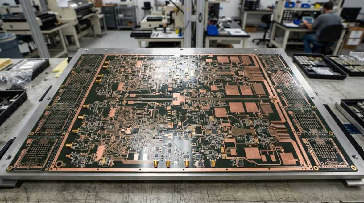
Consider a 16-layer board, 2.8 mm (110 mil) total thickness, with a high-speed differential pair routed on Layer 3. A through-hole via connects a BGA pad on Layer 1 down to the signal layer on Layer 3. The unused barrel continues from Layer 4 through Layer 16—roughly 2.3 mm of stub. Without back drilling, that stub creates a resonant notch around 32 GHz, well inside the third-harmonic band of a 10.3125 Gbps NRZ signal.
Key Stackup Decisions That Affect Back Drill
- Signal-layer placement: Route high-speed nets on layers close to the drill-entry side to minimize stub length before back drilling, or plan a back drill from the opposite side to remove the longer barrel.
- Symmetry: A symmetric stackup simplifies warpage control during lamination and keeps back drill depth consistent across the panel. Asymmetric constructions shift the neutral axis and can cause bow that degrades drill-depth accuracy.
- Dielectric thickness distribution: Thicker cores between non-signal layers give the drill more margin for depth error. Thin cores (< 0.1 mm / 4 mil) near the target layer tighten the tolerance window dangerously.
- Reference plane placement: Ground or power planes immediately below the target signal layer serve as a natural “stop” reference for the drill depth calculation and provide a return-current path for the remaining via segment.
For designs requiring precise impedance targets alongside back drill planning, an impedance table organized by material helps you lock trace geometry before committing the stackup to fabrication.
Back Drill Depth Targeting and Tolerance
The drill must remove the stub without damaging the target signal layer or its adjacent reference plane. The depth is calculated from the entry surface down to a point just past the last unused copper layer, leaving a controlled air gap (back drill clearance) above the target layer.
Depth Budget Breakdown
| Parameter | Typical Value | Notes |
|---|---|---|
| Total board thickness | 2.0–3.2 mm (80–126 mil) | Measured after lamination, not nominal |
| Back drill clearance (air gap) | 0.15–0.25 mm (6–10 mil) | Distance from drill tip to nearest active pad |
| Drill depth tolerance | ±0.05–0.10 mm (±2–4 mil) | Depends on equipment and back drill process control |
| Remaining stub after drill | 0.20–0.35 mm (8–14 mil) | Clearance + tolerance combined |
| Pressed thickness tolerance | ±0.05 mm (±2 mil) | Lamination variation; dominates total budget |
The residual stub length equals the back drill clearance plus the worst-case depth tolerance plus the pressed-thickness tolerance. For a well-controlled process, expect 0.20–0.35 mm (8–14 mil) of remaining stub. At Dk = 4.0, a 0.3 mm stub pushes the quarter-wave resonance above 250 GHz—safely irrelevant for virtually all current digital and RF links.
Pressed thickness variation is the single largest contributor to depth error. Techniques for tightening this, including coupon-based feedback and lamination pressure profiling, are covered in detail under pressed thickness control.
Stub Resonance and Inductance Considerations
A via stub behaves electrically as a shorted transmission-line segment. Its first resonant null appears at fres ≈ c / (4 · Lstub · √Dkeff). At that frequency, the stub presents a near-short to the signal path, creating a deep insertion-loss notch. Even below resonance, a long stub adds excess capacitance and degrades return loss progressively. For a deeper analysis of how stub length maps to specific frequency notches, see our page on via stub resonance.
The remaining via barrel after back drilling also contributes parasitic inductance that affects impedance matching, especially in DDR and SerDes channels. The inductance per unit length of a via barrel depends on the barrel diameter, anti-pad diameter, and surrounding dielectric. Use the calculator below to estimate inductance contribution of the remaining via segment.
For example, a 0.3 mm drill diameter via with a 0.6 mm anti-pad in FR-4 yields roughly 0.7–1.0 nH per millimeter of barrel length. A 0.5 mm remaining stub contributes about 0.4 nH—small, but not negligible when your impedance budget is tight at 25+ Gbps.
DDR and High-Speed Digital: Length Rules Meet Back Drill
In DDR4 and DDR5 memory channels, length matching between data, strobe, clock, and address groups is critical. Via stubs add uncontrolled phase shift that the length-matching rules do not account for. A 1 mm stub difference between two vias in a byte lane can introduce several picoseconds of skew—comparable to the entire length-matching tolerance for DDR5 at 4800 MT/s and above.
Back drilling normalizes the electrical via length across the bus, making your length-matching rules meaningful rather than aspirational. Use the DDR length rule assistant below to check your length budgets against the data rate and topology you are targeting.
If the tool shows your timing margin is under 5 ps, even small stub-length variation matters. In that case, specify back drilling on all DDR via transitions and tighten the pressed-thickness tolerance to ±0.05 mm by requesting lamination coupons measured before drilling. For broader context on how RF and digital length-matching philosophies differ, see length matching in RF versus digital.
Stackup Design Checklist for Back Drill
- Map every high-speed net’s layer transitions. Identify which vias need back drilling and from which side.
- Place signal layers near one surface. This minimizes stub length before drilling and maximizes the drill-entry distance, giving better mechanical control.
- Ensure ≥ 0.20 mm dielectric between the target signal layer and the nearest non-target copper. This provides clearance for drill-tip tolerance.
- Specify pressed-thickness tolerance on the fabrication drawing. Call out ±0.05 mm if your frequency exceeds 15 GHz; reference IPC-6012 Class 3 for rigid-board performance requirements.
- Add back drill coupons. Include test coupons at panel edges with cross-section targets so the fabricator can verify depth before committing production panels.
- Document residual stub spec. State the maximum allowable remaining stub (e.g., ≤ 0.30 mm / 12 mil) on the drill drawing, not just the drill depth.
- Review anti-pad sizing. The back drill hole is typically 0.20 mm (8 mil) larger in diameter than the original plated hole. Ensure anti-pads on all drilled-through layers clear the larger hole to avoid shorting to internal planes.
Common Mistakes
- Ignoring lamination tolerance: A ±0.10 mm pressed-thickness swing doubles your residual stub budget. Always use measured post-lamination thickness, not the nominal stackup drawing value.
- Drilling from the wrong side: If signals route on Layer 14 of a 16-layer board, drill from Layer 1 side. Sounds obvious, but mixed-signal boards with transitions on multiple layers often get this wrong when the drill drawing is auto-generated.
- Forgetting hybrid-material expansion: Mixed-dielectric stackups (e.g., Rogers + FR-4) have different Z-axis thermal expansion rates. After lamination and thermal cycling, the actual layer positions can shift. Account for this in your depth calculation, and consider material selection carefully for boards that combine high-frequency laminates with standard epoxy layers.
FAQ
How short must a via stub be for 28 GHz operation?
For a quarter-wave resonance above 56 GHz (twice the operating frequency, providing margin), the stub must be shorter than about 0.5 mm (20 mil) in FR-4. Back drilling with standard tolerances achieves 0.20–0.35 mm residual stubs, which is sufficient.
Can I avoid back drilling with blind vias instead?
Yes. Blind or buried microvias eliminate stubs entirely. However, they add lamination cycles, cost 30–60 % more than through-hole plus back drill for equivalent layer counts, and introduce registration challenges in boards above 12 layers.
Does back drilling weaken the board mechanically?
The removed barrel no longer provides Z-axis reinforcement at that via location. For boards with dense back-drilled via fields, run a thermal-cycle reliability analysis. IPC-TM-650 2.6.26 (IST testing) is commonly used to validate via reliability after back drilling.
What drill-depth accuracy can I realistically expect?
Modern CNC back drill equipment achieves ±0.05 mm (±2 mil) under controlled conditions. The dominant uncertainty is pressed-thickness variation, not the drill itself. Specifying lamination coupons and measuring actual thickness before drilling is the most effective way to tighten the total budget.
Ready for a quotation?
Send your requirements for a material, stackup and manufacturing review. Price and schedule are confirmed for your project.