

Receiver front ends · Low-noise RF design
LNA PCB design and manufacturing starts with the path before the amplifier. Connector, filter, switch and trace loss can degrade receiver noise performance before active gain is available. Coordinate the RF layout, grounding, assembly and test plan around that requirement.
An LNA PCB carries a low noise amplifier and its RF, bias and support circuitry. Under the matched 290 K model, passive loss before the LNA directly increases the noise figure of that input cascade. Low-loss routing matters, but stability, matching, blockers and assembly also determine whether the receiver performs as intended.
Translate low-noise requirements into board decisions
| Requirement | PCB or assembly consideration | Evidence to request |
|---|---|---|
| Low receiver noise figure | Loss before LNA, input match and grounding | Calibrated assembled measurement at defined planes |
| Gain and stability | Bias decoupling, feedback paths and layout | Wide enough frequency and operating-condition checks |
| Input/output match | Stackup, trace geometry and launches | Model and measured S-parameters where required |
| Repeatability | Material, copper, component and assembly control | Approved revision and traceable build information |
| Blocker handling | Front-end filters, supply behavior and device choice | Circuit-specific linearity and operating tests |
LNA cascade noise figure calculator
Uses Friis noise factor addition with matched stages and passive input loss at the reference temperature of 290 K. Gain refers to the LNA alone. Input loss can include a filter, switch, connector and PCB trace. The model excludes mismatch, blockers, nonlinear behavior and noise-wave correlation.
Why the path before the amplifier is important
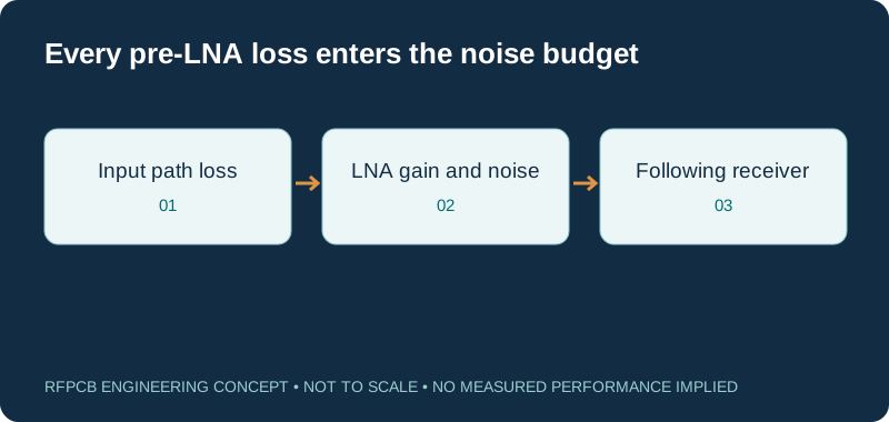
Passive input loss reduces the available signal before the amplifier can add gain. In the matched reference-temperature model used here, that loss adds directly to the noise figure of the input loss plus LNA combination. It can include more than the PCB trace: connectors, filters, switches and transitions may all contribute.
Make a block diagram with the physical order of these elements and record the measurement reference planes. Reducing a loss after substantial gain has a different effect on cascade noise from reducing the same loss before the first amplifier. The placement of each element matters as much as its individual specification.
Use the cascade noise calculator as a budget model
Enter the passive loss before the LNA, the LNA noise figure and gain, and the noise figure of the following receiver stage. The tool converts decibel inputs to linear factors and applies the Friis cascade relationship. Its reported net gain is the input loss plus LNA gain, before the following stage.
The assumptions are matched stages, small-signal operation and a passive input network at 290 K. Mismatch, noise-wave correlation, compression and blocker effects are excluded. A plausible result is useful for a budget discussion but does not certify the assembled receiver or replace a calibrated noise measurement.
Choose the material for the actual input path
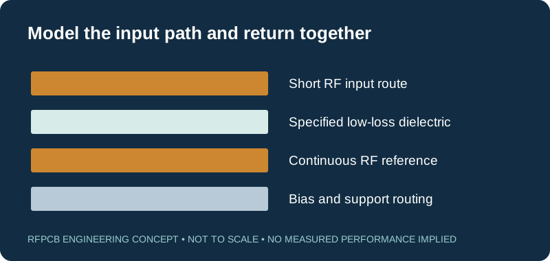
The useful material decision depends on frequency, path length, geometry and allowed loss. A very short connection and a longer front-end network can justify different constructions. Compare exact material and copper options instead of selecting the lowest headline Df without considering the rest of the circuit.
Use the RF material selection guide and the RO3003 versus RO4350B comparison to prepare candidates. Keep the selected stackup and reference plane consistent with the layout model and manufacturer reference design.
Treat matching and minimum noise as different objectives
An input match chosen for a particular noise performance is not automatically the same condition as a perfect power match. Follow the amplifier manufacturer guidance and use the relevant device data when designing matching networks. Component parasitics and layout can influence the result at RF.
If tuning is expected, identify the permitted component options and measurement process. Preserve the final BOM and placement configuration after acceptance. A board assembled with an earlier matching network should not be expected to reproduce measurements from a later tuned prototype.
Maintain ground and supply discipline
Input and output coupling, shared return paths and supply feedback can affect stability and repeatability. Review grounding around the amplifier, matching components and connector launches. Keep the RF return path intentional and account for the placement and connection of decoupling components.
Copying only the visible outline of a reference layout can miss important layer and via details. Record the proposed construction and compare it with the reference design assumptions. Changes made for routing convenience or component availability should be reviewed for their effect on the complete circuit.
Check stability beyond the intended passband
An amplifier can have unwanted behavior outside the operating band, so a narrow in-band gain result is not a complete stability assessment. The relevant checks depend on the device, bias, load and surrounding network. Follow the component manufacturer recommendations and the project validation plan.
Manufacturing should reproduce the approved layout and assembly details rather than silently changing them. If the board includes a shield, enclosure or cable interface, include those conditions in the test definition. The bare PCB supplier cannot establish amplifier stability from laminate identity or continuity testing alone.
Coordinate assembly with the RF design
Provide a controlled BOM, component orientation and placement data, soldering requirements and any shield or connector instructions. Device variants and matching-component substitutions can affect the RF response, even if their nominal labels look similar. Identify parts that require engineering approval before substitution.
The RF assembly page explains the information needed for a populated-board request. Define whether the supplier provides assembly only or also bias checks, gain measurements, noise measurements or another functional test. Separate those deliverables clearly in the quotation.
Measure noise figure with known reference planes
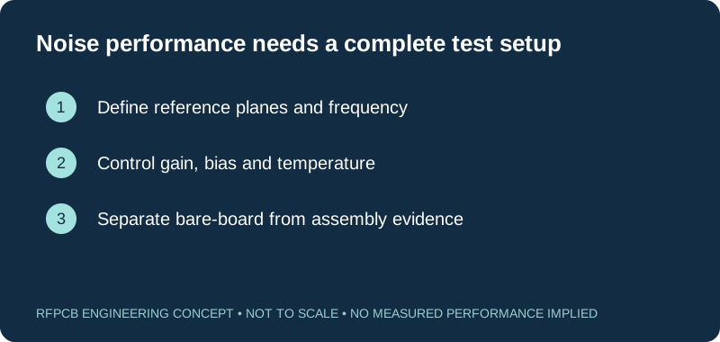
Specify the frequency range, bias condition, temperature assumptions and the interfaces included in the result. Calibration, fixture loss and mismatch can influence interpretation. State whether the acceptance target refers to the amplifier board input, a connector ahead of a filter or the complete receiver input.
Keep the noise budget and measured result referenced to the same location. If a connector or input fixture is de-embedded, document the method and assumptions. A lower displayed number is not necessarily an improvement if the measurement boundary changed between samples.
Prepare a manufacturing and validation handoff
Send the fabrication files, stackup, exact material and finish, assembly data and the required quantity. Mark the RF-sensitive input path and any controlled geometry. Include the expected bias and test interfaces when requesting assembled measurements, and identify who supplies fixtures or calibrated test equipment.
Use the RF DFM checklist to expose missing inputs. For a front end containing a filter or duplexer, review that network alongside the amplifier rather than treating it as a zero-loss accessory. The accepted product should have one controlled revision linking board, BOM and test requirements.
Prepare a reviewable engineering request
Check only the requirements you have actually documented. This list records readiness; it does not inspect your files or certify a design. Missing information is useful: identify it explicitly so the engineering review can resolve it before a production release.
These inputs are processed in your browser and are not submitted by this tool. The downloaded summary is a plain-text planning record. Use the secure quote form to send files; request an NDA first if your project requires one.
Manufacturing context
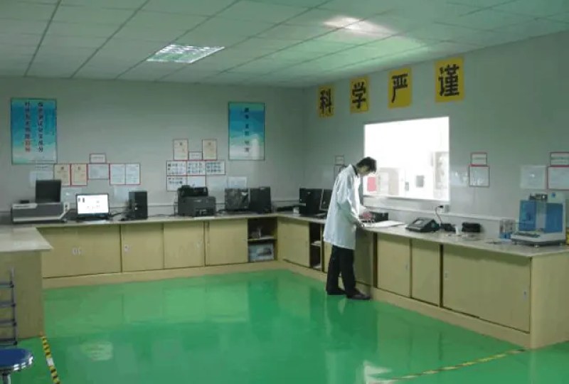
RFPCB and PCBSync share the manufacturing facility shown below. These process photographs illustrate the production environment; they are not evidence that a particular board, material grade or RF performance has been qualified. Request the documentation and inspection scope applicable to your project.


LNA PCB FAQs
Does one decibel of input loss add one decibel of noise figure?
For a matched passive input network at 290 K ahead of the LNA, its loss adds to the noise figure of that input cascade. Other temperatures, mismatch and more complex networks need an appropriate model. The full receiver also includes later-stage contributions.
Can low-loss laminate alone guarantee a low noise figure?
No. Input-path loss, device behavior, matching, layout, grounding, bias and assembly all contribute. The laminate is one part of the construction. Validate the assembled circuit at clearly defined reference planes.
Does the calculator predict stability or blocker performance?
No. It is a small-signal noise cascade model. It does not calculate oscillation risk, compression, intermodulation or behavior under strong blockers. Those require device-specific analysis and the relevant circuit tests.
What is needed for an LNA PCB assembly quote?
Provide the fabrication package, approved stackup, BOM, placement files, assembly notes and test scope. Include matching variants, connectors, shields and bias conditions. State whether noise figure and other RF measurements are required deliverables.
Continue your engineering review
Request an LNA board or assembly review
Share the input-loss budget, stackup and controlled BOM with the intended measurement boundaries. Specify whether you need bare boards, assembly or defined RF test results.
Sources and engineering scope
- Analog Devices: input loss and high-frequency LNA stability
- Analog Devices: LNA matching and noise-figure tradeoffs
- Rogers RO4000 manufacturer datasheet
Manufacturer values apply to the identified grade, test method and construction. Engineering examples on this page are illustrative; they are not measured product results, inventory statements or certification claims. Rogers product names are trademarks of their owner. Keep the applicable datasheet revision with your approved manufacturing package.
Related engineering decisions
Ready for a quotation?
Send your requirements for a material, stackup and manufacturing review. Price and schedule are confirmed for your project.