

Engineering terminology · Clear specifications
This RF PCB glossary explains terms that connect circuit design, bare-board manufacturing and purchasing. Each definition includes the distinction that matters when writing a drawing or reading a supplier response. Use the checklist to identify which parts of your project specification still need a shared definition.
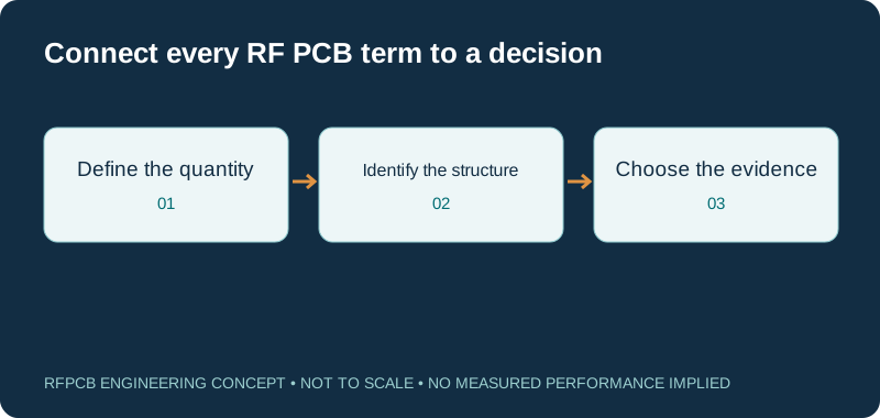
A useful RF PCB requirement identifies the material and geometry, the quantity being controlled, and the evidence used to verify it. Dk is not impedance, Df is not insertion loss, a continuity result is not an RF test, and a material lot number is different from measurement traceability. The definitions below explain those boundaries.
Common terms that answer different questions
| Terms | Useful distinction | Record in the specification |
|---|---|---|
| Process Dk / design Dk / effective permittivity | Material test reference, modeling reference and guided-structure behavior | Method, frequency and applicable model |
| Df / insertion loss | Dielectric-loss parameter versus loss of a circuit path | Units, operating band and measurement boundaries |
| Core / prepreg / bondply | Structural dielectric and materials used to bond a stack | Named grades and finished layer separations |
| Starting copper / finished copper | Cladding before processing versus resulting conductor | Thickness location, tolerance and plating scope |
| TDR / VNA / continuity test | Time-domain reflection, frequency-domain network behavior and connectivity | Which result verifies which requirement |
| Lot traceability / metrological traceability | Material genealogy versus reference chain for a measurement result | Identifiers, linked records and uncertainty context |
RF PCB, bare board and assembly
RF PCB describes a printed circuit board whose intended function involves radio-frequency signals. The label alone does not establish a frequency limit, laminate family, layer count or testing scope. Microwave and millimeter-wave describe frequency regions, but a procurement requirement should state the actual operating band rather than relying on those broad labels.
Bare board means the fabricated interconnect before component assembly. A PCB assembly includes mounted components and the associated assembly work. Specify which article a test applies to: a bare transmission-line coupon, a board with connectors, or a populated circuit can produce different evidence. The RF PCB assembly guide helps define where fabrication ends and the additional assembly scope begins.
Laminate, core, prepreg and bondply
Laminate is a manufactured dielectric sheet or composite; copper-clad laminate includes attached copper foil. A core is an already consolidated dielectric layer, often clad, used in a board construction. Prepreg commonly refers to reinforcement impregnated with resin that flows and cures during lamination. Its grade, glass construction and resin content help determine the finished dielectric region.
Bondply names a bonding material, but the term does not by itself identify one chemistry or reinforcement. Rogers supplies both reinforced prepreg products and an unreinforced 2929 bonding film. Keep the exact product designation in the stackup. Pressed thickness is the resulting spacing after the bonding process; it need not equal the unpressed sheet thickness. Copper distribution and the chosen process matter when defining that final dimension.
PTFE, thermoset and reinforcement
PTFE, polytetrafluoroethylene, is a fluoropolymer used in some RF laminates. A PTFE-based material may also contain ceramic filler and glass reinforcement. Thermoset describes a resin system that forms a crosslinked network during cure. Material brands can include products from different chemistry families, so a manufacturer name cannot substitute for a grade designation.
Reinforcement supports the composite mechanically; its form may include woven glass. Filler is another constituent used to modify material behavior. “Ceramic-filled” does not mean the PCB substrate is a solid ceramic plate. Read composition and processing guidance together, especially when considering bonding and plated-hole preparation. The PTFE versus hydrocarbon comparison explains why similar electrical numbers do not establish identical fabrication routes.
Dk, process Dk, design Dk and effective permittivity
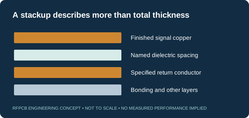
Dk is a common industry label for relative dielectric permittivity. It is dimensionless and depends on the material response, frequency and measurement context. Process Dk identifies a reference from a specified material test. Design Dk is a separately characterized reference used to support circuit modeling; the source must identify its method and applicability.
Effective permittivity describes propagation in a particular guided structure, including the field's surrounding media. It is not automatically either material Dk entry. Rogers' Dk measurement explanation discusses why reported values differ between methods. Preserve the labels when exchanging simulation inputs. Averaging process and design Dk, or treating their difference as a lot tolerance, confuses different quantities.
Df, attenuation, insertion loss and return loss
Df, dissipation factor or dielectric loss tangent, is a dimensionless material-loss parameter under specified conditions. Attenuation per unit length describes distributed loss in a defined transmission line at a stated frequency. Insertion loss concerns transmission through a path; for the usual matched, equal-real-reference-impedance two-port convention it is −20 log₁₀|S21| in dB.
Return loss describes reflection: −20 log₁₀|S11| in dB for the input port under the applicable termination conditions. Thus S11 displayed as −20 dB corresponds to positive 20 dB return loss. Lower insertion loss and higher positive return loss generally indicate different desirable behaviors for a passive transmission path. Neither quantity alone identifies whether loss arose in dielectric, copper or a transition.
Copper weight, roughness and final finish
Copper weight is a foil mass-per-area convention commonly used to describe nominal cladding thickness. Starting copper and finished copper differ when processing adds plating or removes metal. Specify the location and basis of the requested thickness, particularly where external traces and plated holes have different requirements.
Copper roughness describes surface texture, with different metrics representing different aspects of that texture. A roughness number without its metric and measured interface is incomplete. Final finish is the surface treatment applied to exposed conductors for the intended assembly or contact needs. Finish is distinct from base foil. Rogers' material and fabrication discussion connects conductor conditions with loss and phase, which is why these details belong beside the dielectric model.
Stackup, impedance and transmission-line structure
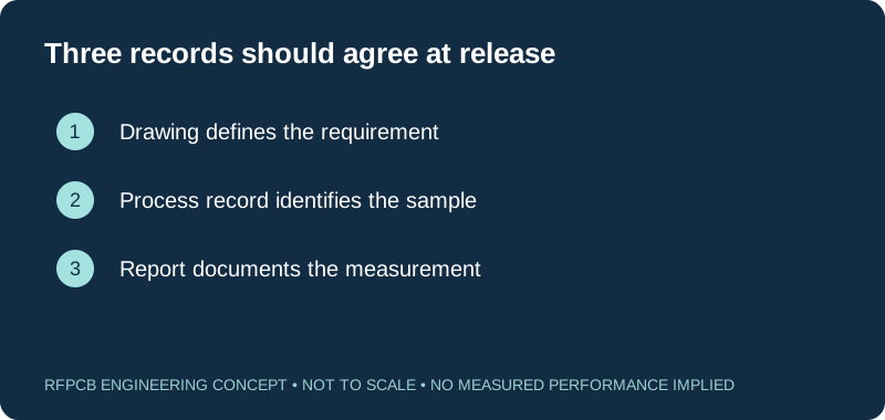
Stackup is the ordered construction of conductor and dielectric layers, including their materials and dimensions. Characteristic impedance describes the voltage-to-current relationship of a traveling wave on a transmission line; it is not the DC resistance measured end to end. A controlled-impedance requirement needs defined geometry, target, tolerance and verification scope.
Microstrip uses a surface conductor with a reference plane separated by dielectric. Stripline embeds the signal between reference conductors. Grounded coplanar waveguide includes adjacent ground conductors and a backing reference plane. Return path describes how the signal's return current travels through the structure. These names guide modeling, but actual dimensions, masks, gaps and transitions remain necessary. Use the stackup library to organize the cross-section.
Vias, plated through holes, stubs and back drilling
A plated through hole spans the board and has a conductive barrel. A blind via connects an outer layer to an internal layer, while a buried via connects internal layers without reaching an outer surface. Microvia denotes a small, short interconnect structure governed by the applicable design and qualification definition; the word alone does not specify a universal size or an approved process.
A via stub is the unused part of a conductive via structure beyond the required connection. Back drilling removes a selected portion of that barrel with a controlled-depth operation. Specify the drill direction, layers to preserve, clearance and allowable residual structure. The cavity and back-drill guide helps translate the intent into reviewable geometry.
Aspect ratio, annular ring and registration
Aspect ratio compares a hole's relevant depth with its diameter. The drawing must establish which diameter convention is intended. For a microvia, use the traversed dielectric depth rather than total board thickness; taper and the landing structure need their own review. An arithmetic ratio does not establish manufacturing feasibility.
Annular ring is the copper surrounding a hole within its pad. For ideal concentric circles, nominal radial ring is half the difference between pad and hole diameters. Registration is the alignment of features such as layers and drilled holes. Actual remaining ring depends on those offsets and manufacturing allowances. A pad calculation therefore cannot replace inspection criteria. For edge connections, a castellation additionally involves a plated hole intersected by the board edge.
Coupon, microsection and first article
A coupon is a test structure intended to represent selected aspects of a board or manufacturing process. Its usefulness depends on what it reproduces: material stack, feature sizes, plating or the electrical route. A coupon is not automatically representative of every feature on the product.
A microsection is a prepared cross-section used to inspect internal construction. IPC's microsection method addresses specimen preparation and the structures to be evaluated. The applicable performance specification supplies acceptance requirements. First-article inspection is an initial verification activity against a defined release package; specify its actual deliverables instead of assuming the phrase includes all RF tests. One report does not by itself establish recurring process performance across later lots.
Continuity, TDR, VNA and S-parameters
Continuity and isolation testing checks intended connections and unintended conductive paths under the selected method. TDR, time-domain reflectometry, evaluates reflections versus time and can support an impedance profile. Its interpretation depends on rise time, fixtures, reference conditions and the tested structure.
A VNA, vector network analyzer, measures complex network behavior across frequency. S-parameters describe traveling-wave relationships at defined ports: S11 concerns input reflection, while S21 concerns forward transmission under specified reference impedances and terminations. Phase is part of the complex result, not an optional synonym for magnitude. Keysight's measurement-parameter documentation explains the port relationships. Define the required test explicitly; “electrically tested” does not tell purchasing which of these measurements is included.
Calibration, reference plane and de-embedding
Calibration establishes measurement corrections or relationships using defined references and procedures. A reference plane identifies the boundary at which a network result is interpreted. A connector, cable or fixture beyond that boundary can remain part of the measured device unless the measurement procedure accounts for it.
De-embedding mathematically removes a characterized fixture network from a measurement. It requires an appropriate fixture representation and consistent ports; it is not a generic smoothing operation. Keysight's fixture-removal guide explains this distinction. Record the calibration and fixture treatment with the data. Comparing raw measurements against de-embedded measurements without aligning the boundaries can produce a misleading material or supplier comparison.
Lot traceability, measurement uncertainty and tolerance
Lot traceability connects material and production identifiers through receiving, processing and delivery. Metrological traceability concerns a measurement result's documented calibration chain to a reference, including uncertainty contributions. NIST emphasizes that traceability belongs to the result; a calibrated instrument alone does not establish everything needed for the later measurement.
Measurement uncertainty characterizes the dispersion of values attributable to the measured quantity within the stated evaluation. Tolerance is the allowed requirement interval. They serve different purposes. A decision rule specifies how measurement uncertainty is considered when deciding conformity. Record that agreement when results approach a limit. A supplier report should identify both the requirement and the measured evidence rather than substituting an unexplained “pass” for the comparison.
RFQ, DFM, CoC, deviation and change notice
An RFQ, request for quotation, defines the requested technical and commercial scope. DFM, design for manufacturability, reviews how the proposed design can be fabricated and which issues need resolution. An approved deviation authorizes a specifically bounded departure; it should identify the affected revision, quantity or period and the acceptance authority.
A CoC, certificate of conformity, is a supplier declaration against stated requirements. It is different from a detailed measurement report. A product or process change notice communicates a proposed or implemented change according to the agreed rules; notification and approval are different actions. Keep the exact standards and revisions in procurement documents. IPC-6018 concerns high-frequency printed-board qualification and performance, but merely naming it does not establish a supplier's compliance or define every project-specific RF limit.
Prepare a reviewable engineering request
Check only the requirements you have actually documented. This list records readiness; it does not inspect your files or certify a design. Missing information is useful: identify it explicitly so the engineering review can resolve it before a production release.
These inputs are processed in your browser and are not submitted by this tool. The downloaded summary is a plain-text planning record. Use the secure quote form to send files; request an NDA first if your project requires one.
Manufacturing context
RFPCB and PCBSync share the manufacturing facility shown below. These process photographs illustrate the production environment; they are not evidence that a particular board, material grade or RF performance has been qualified. Request the documentation and inspection scope applicable to your project.



RF PCB terminology questions
Does controlled impedance mean the board has low RF loss?
No. Impedance and attenuation are different quantities. A line can meet an impedance requirement while its length, conductor system or dielectric loss produces more attenuation than the application permits.
Are prepreg and bondply always the same material?
No. Product naming varies and bonding materials may use different reinforcement and chemistry. Specify the exact grade and finished construction rather than relying on either category word alone.
Does a certificate of conformity include VNA measurements?
Only if the agreed deliverable explicitly includes those measurements and the linked report. A declaration of conformity is not automatically a dataset containing frequency response, sample identity and reference-plane details.
Which definitions should appear on a purchase order?
Include the definitions needed to remove ambiguity from the actual requirement: material identity, construction, dimensional basis, acceptance methods, applicable standard revisions, report scope and change-approval rules. The glossary supports that agreement; it is not a replacement for it.
Continue your engineering review
Resolve ambiguous requirements before release
Attach your stackup and fabrication notes, then identify terms that need clarification. A useful engineering response connects each requirement to the proposed construction and the evidence that will verify it.
Sources and engineering scope
- Rogers: Managing PCB Materials Dielectric Constant (Dk)
- Rogers: Understanding Material Interactions with PCB Fab Processes
- Rogers: 2929 Bondply multilayer processing guidance
- Rogers: RO4450F and RO4460G2 reinforced bondply/prepreg datasheet
- Keysight: S-parameter measurement definitions and port relationships
- Keysight: High Precision Time Domain Reflectometry
- Keysight: Removing Unwanted Effects from the Measurement
- NIST: Metrological Traceability, Frequently Asked Questions and Policy
- IPC-TM-650 2.1.1F: Microsectioning specimen preparation
- IPC-6018D official table of contents: high-frequency printed-board qualification and performance scope
Manufacturer values apply to the identified grade, test method and construction. Engineering examples on this page are illustrative; they are not measured product results, inventory statements or certification claims. Manufacturer and product names belong to their respective owners. Keep the applicable datasheet revision with your approved manufacturing package.
Ready for a quotation?
Send your requirements for a material, stackup and manufacturing review. Price and schedule are confirmed for your project.