

PLL and local oscillator boards · Noise-aware construction
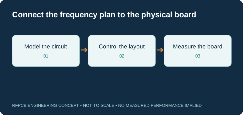
Frequency synthesizer PCB design connects the reference source, PLL, oscillator, power network and output interface into one physical circuit. Prepare the board construction alongside the frequency plan, then use measured hardware to verify noise, spurs and tuning behavior.
A frequency synthesizer PCB needs a defined RF construction, controlled coupling around sensitive nodes and a repeatable acceptance setup. The tool below converts already integrated single-sideband phase noise into RMS phase error and time jitter; it does not design a PLL loop filter or predict board performance.
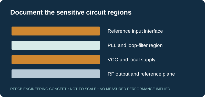
PLL board regions and their manufacturing review inputs
| Circuit region | What to identify | Evidence to keep |
|---|---|---|
| Reference input | Source, interface, route and termination | Input conditions used for the measurement |
| PLL and loop filter | Selected parts, values and sensitive routing | Simulation revision and populated BOM |
| VCO and supply | Power network and approved local layout | Supply conditions and operating state |
| RF output path | Band, impedance, connector and reference plane | Output measurement setup and fixture data |
| Control interface | Programming sequence and active bus conditions | Firmware or register-set revision |
| Acceptance report | Offsets, integration limits and spur treatment | Instrument settings and board identity |
Integrated phase noise to jitter
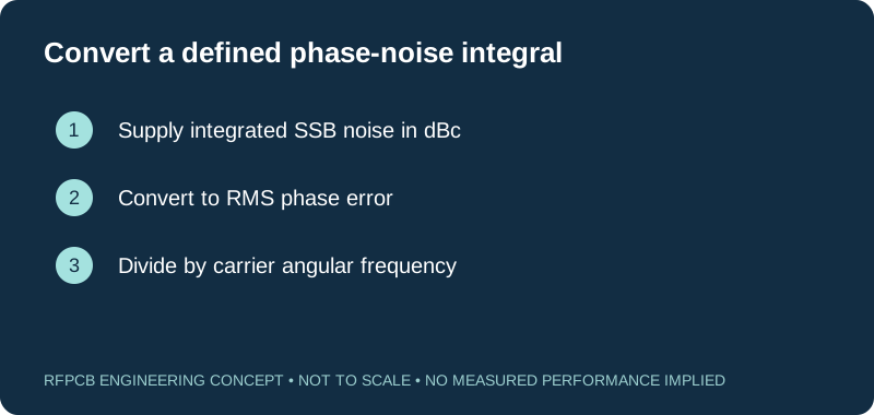
Supply integrated SSB noise L in dBc, already integrated over the specified offset interval. A single spectrum point in dBc/Hz cannot be entered directly. RMS phase = √(2 × 10^(L/10)) radians; RMS jitter = phase/(2π × carrier frequency). The interval records your integration scope; this tool does not integrate a spectrum. Small phase-error model; identify whether discrete spurs are included.
Define the frequency plan and the acceptance question
List the output range, channel settings, reference source and operating states before discussing PCB fabrication. A local oscillator for a receiver and a sampling clock can share synthesizer technology while needing different acceptance reports. State whether your priority is noise at selected offsets, an integrated jitter figure, discrete spurs, settling behavior or several independent limits.
Attach that list to the design review. Identify the settings and frequency transitions requiring evaluation. A test at one convenient channel does not establish behavior across the full plan.
Preserve the model and the exact component implementation
Analog Devices recommends simulation followed by hardware verification in its PLL design and debugging guide. Its guidance includes realistic reference and VCO models and review of actual loop-filter component values. Keep the simulation file, schematic and populated BOM together so those assumptions can be compared.
Identify substitutions needing circuit review. Evaluate an alternative against the properties important to its role, beyond nominal value and package. Record prototype tuning in the released BOM so later builds include approved bench changes.
Treat sensitive placement as a controlled design feature
The ADI guide highlights VCO supply sensitivity, compact loop-filter placement and separation of digital activity from reference and RF output paths. Use these principles with the selected device documentation, then mark the relevant regions on an annotated layout. Do not turn them into a universal dimensional rule for unrelated devices.
Give fabrication and assembly reviewers enough context to recognize consequential changes. Identify prohibited copper additions or routing edits where the circuit model depends on a particular geometry. If a supplier requests a pad or via adjustment, return the question to the circuit owner with the changed area visible rather than approving it as an isolated drawing edit.
Specify an RF construction where it is actually needed
The highest output frequency is only one input to the construction choice. Identify the length and geometry of RF output paths, their loss and phase requirements, and any transitions that need modeling. A short integrated synthesizer layout and a board with distributed output filtering can justify different material decisions.
If a thermoset RF laminate is a candidate, use the RO4350B material guide to organize the specification. The impedance calculator provides an initial geometry aid. Confirm the actual dielectric, copper, finish and reference-plane arrangement with manufacturing before freezing controlled routes.
Use integrated phase noise with the correct units
The input L is integrated single-sideband phase-noise power in dBc over an offset interval you have already selected. It is not a single spectral-density reading in dBc/Hz. Under the small-phase-error assumption, σφ = √(2 × 10^(L/10)) radians. Convert radians to degrees by multiplying by 180/π, and time jitter is σφ/(2πf), with carrier f in hertz. These relationships follow ADI tutorial MT-008.
The tool accepts carrier frequency in MHz and reports time in picoseconds. It does not integrate a spectrum, choose an offset interval, synthesize component values or assess loop stability. Record the supplied integral and its limits in the project notes.
Interpret the result as a conversion, not a noise prediction
As an arithmetic example, −60 dBc integrated SSB noise at a 100 MHz carrier corresponds to approximately 0.081 degrees RMS phase error and 2.25 ps RMS time jitter. These are calculated values from the stated input, not measured results for a PCB. At the same integrated phase error, doubling the carrier frequency halves the converted time jitter.
When comparing reports, keep integration limits and treatment of discrete spurs consistent. Also identify the carrier output and operating configuration behind each value. A smaller result obtained with a different measurement scope cannot establish that one board implementation is better. Preserve the spectrum or original report alongside the converted number.
Include the downstream load and output interface
Describe the load connected to each synthesizer output during operation and during acceptance testing. Identify buffers, splitters, filters, cables and connectors included in the result. For a receiver local oscillator, coordinate the required interface with the receiver team; the LNA PCB guide provides context for the surrounding receive path.
Use the filter and duplexer guide when an output network adds a separate manufacturing-sensitive RF structure. Mark the measurement reference plane on the test drawing. A result at an evaluation connector should not silently become the claimed result at a different point inside the assembled product.
Make bring-up and acceptance measurements repeatable
Create a test record that includes board identity, firmware or register configuration, reference source, supply settings, output connection and instrument setup. Separate a successful lock indication from the noise, spur and settling measurements required by the specification. A lock flag alone is not the complete acceptance result.
Decide how test equipment will connect without unintended loading of sensitive nodes. Label connectors and document temporary test components. Record bench modifications and whether they remain in production. Preserve unsuccessful conditions too; they help define the limits of the approved configuration.
Quote the fabrication and verification scopes separately
Send the proposed stackup, artwork, controlled-impedance requirements and critical dimensions as one package. List any additional assembly or RF measurement work explicitly so it can be reviewed and priced. Standard bare-board electrical testing does not measure synthesized phase noise or establish a finished module’s jitter.
Use the RF PCB cost calculator to compare the documented scope, then send the files through the quote form. Include quantities, required evidence and rules for material or component changes. A reviewed quotation should make clear which results will be delivered and which remain part of your own system validation.
Prepare a reviewable engineering request
Check only the requirements you have actually documented. This list records readiness; it does not inspect your files or certify a design. Missing information is useful: identify it explicitly so the engineering review can resolve it before a production release.
These inputs are processed in your browser and are not submitted by this tool. The downloaded summary is a plain-text planning record. Use the secure quote form to send files; request an NDA first if your project requires one.
Manufacturing context
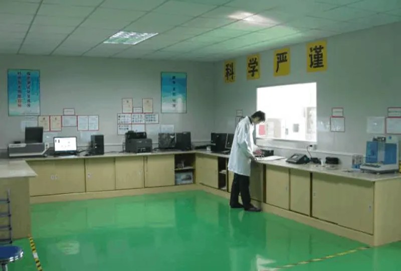
RFPCB and PCBSync share the manufacturing facility shown below. These process photographs illustrate the production environment; they are not evidence that a particular board, material grade or RF performance has been qualified. Request the documentation and inspection scope applicable to your project.


Frequency synthesizer PCB FAQs
Does this calculator design the PLL loop filter?
No. It converts integrated phase-noise power to RMS phase error and time jitter. Loop-filter design requires the selected PLL, oscillator, reference, loop requirements and an appropriate circuit model, followed by verification of the actual implementation.
Can I enter a phase-noise reading in dBc/Hz?
No. A reading at one offset is a spectral density, not the integrated noise power requested here. Obtain the integrated single-sideband value in dBc for your chosen offset interval, and record the interval and spur treatment alongside it.
Does a low-loss laminate guarantee low phase noise?
No. The board construction is one part of a complete synthesizer. Source quality, selected components, power, coupling, configuration and the measurement setup all matter. Material selection cannot replace circuit analysis and assembled-board verification.
Is a locked PLL ready for acceptance?
A lock indication is one check. The board still needs the measurements required by its specification, such as output frequency, spurs, phase noise and settling. Record the configuration and test conditions so later builds can be compared meaningfully.
Continue your engineering review
Prepare a reviewable frequency synthesizer PCB request
Send the frequency plan, stackup, critical routing and required acceptance evidence. Include the intended test interfaces and distinguish bare-board fabrication from assembled-circuit verification.
Sources and engineering scope
- Analog Devices: How to Design and Debug a Phase-Locked Loop Circuit
- Analog Devices MT-008: Converting Oscillator Phase Noise to Time Jitter
Manufacturer values apply to the identified grade, test method and construction. Engineering examples on this page are illustrative; they are not measured product results, inventory statements or certification claims. Manufacturer and product names belong to their respective owners. Keep the applicable datasheet revision with your approved manufacturing package.
Ready for a quotation?
Send your requirements for a material, stackup and manufacturing review. Price and schedule are confirmed for your project.