
RF applications · Test fixtures and measurement paths
A test and measurement PCB is part of the measurement system: its launches, traces, switching paths and mechanical support can affect the result attributed to the device under test. Define which parts belong inside the measured path before selecting the laminate or finalizing the fixture.
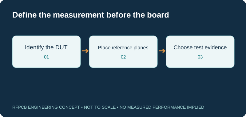
Specify the operating band, test article, electrical reference planes and repeatable connection method first. Then release a controlled stackup and inspection plan. Bare-board DC testing, TDR impedance checks, VNA measurements and microsections provide different evidence; agree which are required and who performs each one.
Choose evidence for the question you need answered
| Method | Useful evidence | Scope that must be stated |
|---|---|---|
| DC electrical test | Continuity and isolation against the intended netlist | Netlist revision, test conditions and board coverage; no RF loss claim |
| TDR | Impedance versus electrical distance on a chosen structure | Coupon or actual net, rise time, launch and evaluation window |
| VNA | Frequency-dependent reflection and transmission | Ports, band, calibration, reference planes and fixture treatment |
| Microsection | Local cross-sectional construction evidence | Section location, sample identity and agreed dimensional features |
| Mechanical inspection | Fit, alignment and selected dimensions | Datums, connector locations, support features and sample plan |
Return loss, VSWR and mismatch
For a passive interface, |Γ| = 10^(−RL/20); reflected power = |Γ|²; VSWR = (1+|Γ|)/(1−|Γ|); mismatch loss = −10 log10(1−|Γ|²). Enter positive return loss, for example 20 dB when S11 is −20 dB. This is a single-interface matched-source interpretation, not total S21 or radiated efficiency.
Define the fixture boundary before choosing material
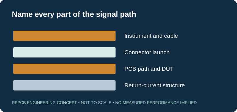
A fixture can connect an instrument to a removable device, carry an evaluation circuit, or route signals through a switching assembly. Those jobs place different demands on loss, isolation, access and service life. Start with a block diagram that names the device, cables, connectors, PCB paths and any components installed between the instrument and the device.
For each result, mark where its reference planes lie. A connector-to-connector measurement includes different structures from a result corrected to device pads. Make this boundary visible in the purchase specification and laboratory procedure.
Design connector launches as part of the RF path
The connection between a coaxial connector and a planar trace is a transition with geometry of its own. Review the connector drawing against board thickness, pad shape, nearby grounds and enclosure clearance. Keep mounting holes and tool access in the mechanical model so an apparently sound RF layout can actually be assembled and serviced.
Consider how the return current crosses the launch and follows the signal into the board. A nearby ground plane is useful only when the transition connects to it appropriately. Define connector assembly and handling instructions with the responsible team. Repeated disconnection should trigger an inspection or maintenance decision instead of silently changing the measurement baseline.
Control the construction used for correlation
Select material from the required electrical and mechanical behavior rather than an instrument frequency label alone. A short adapter and a long phase-sensitive path may justify different constructions. Keep dielectric spacing, conductor geometry, copper type and finish in the simulation inputs and manufacturing drawing so the model describes the intended board.
Identify which dimensions matter to the comparison, including launch openings, coupled gaps and reference-plane interruptions. Use the RF PCB DFM checklist to resolve ambiguous notes before release.
Separate calibration from fixture correction
Keysight describes de-embedding as removing a characterized fixture contribution to place results at the intended device interface. Keep the raw measurement, fixture description and correction settings together. A corrected plot without its model or reference-plane definition is difficult for another engineer to reproduce.
Decide which structures can be measured directly and which require mathematical correction. Reserve access and any agreed characterization structures in the layout before the panel is finalized. Inspect unexpected features in both raw and corrected results; do not assume correction makes a poor connection harmless. Record the validation used to support the chosen correction method and repeat that review when the fixture construction changes.
Use return loss without confusing it with total path loss
The interactive tool accepts positive return loss in decibels. It calculates reflection magnitude as 10 raised to minus return loss divided by twenty, then converts that magnitude to reflected power percentage and VSWR. Single-interface mismatch loss is minus ten times the base-ten logarithm of one minus reflected power fraction.
For an illustrative 20 dB input, reflected power is 1%, VSWR is about 1.222, and this mismatch loss is about 0.044 dB. These numbers describe one idealized interface. They do not predict aggregate S21, antenna radiation efficiency or a chain of interacting discontinuities. Enter 20 for a return loss corresponding to an S11 log-magnitude display of minus 20 dB.
Assign each test to an owner and a sample
A bare board can pass a DC netlist test while an assembled fixture still has an unacceptable RF transition. Likewise, a TDR coupon result does not automatically cover every connector launch or switching path. Specify whether each check applies to all delivered boards, selected boards, panel coupons or a separately assembled qualification unit.
RFPCB and PCBSync share the manufacturing facility whose general rigid-board capability information includes electrical testing, TDR and microsection. Confirm the scope for the submitted construction. Do not infer an included VNA sweep, laboratory accreditation or finished-fixture calibration from that general list. Use the test report guide to request distinct records.
Preserve repeatability through mechanical design
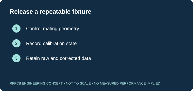
A fixture that flexes during mating can change its connections and stress solder joints. Place support where assembly loads occur and keep the support scheme consistent during measurement. Define board location with deliberate datums instead of relying on the edges of an uncontrolled enclosure opening. Include access for cleaning and visual inspection where repeated connections occur.
For fixtures with multiple paths, identify every port physically and in the data file. A swapped label can invalidate an otherwise careful comparison. Establish a baseline after assembly, record maintenance or connector replacement, and decide when the fixture must be rechecked. These controls belong to the fixture workflow, not just the PCB artwork.
Quote the fixture and its validation separately
Separate bare-board fabrication from connectors, assembly, characterization structures, laboratory time and documentation. Ask which items are included in the proposal and which remain with your engineering team. A fixture ordered for an early feasibility experiment may need a different sample quantity and documentation package from a production test station.
Use the RF PCB cost planner to expose these budget assumptions without treating its example values as supplier prices. Reserve space for coupons and handling rails before estimating panel utilization. Include the expected number of test connections and any spare fixtures in the purchasing discussion; the least expensive bare board may not minimize the cost of maintaining repeatable tests.
Release a package another laboratory can understand
Deliver a consistent board revision, stackup, connector list, port map and test specification. Include the operating band, sweep requirements, relevant environmental conditions and the raw data format you need. State whether connectors and fixture paths remain in the reported result. Keep illustrative calculations separate from measured acceptance records.
When the first articles arrive, link each measurement to the physical sample and preserve the setup configuration. Investigate differences against the agreed boundary before attributing them to laminate or manufacturing variation. For repeat builds, define which changes require renewed correlation. A useful fixture record should let another engineer reconstruct what was measured and identify what the result does not cover.
Prepare a reviewable engineering request
Check only the requirements you have actually documented. This list records readiness; it does not inspect your files or certify a design. Missing information is useful: identify it explicitly so the engineering review can resolve it before a production release.
These inputs are processed in your browser and are not submitted by this tool. The downloaded summary is a plain-text planning record. Use the secure quote form to send files; request an NDA first if your project requires one.
Manufacturing context
RFPCB and PCBSync share the manufacturing facility shown below. These process photographs illustrate the production environment; they are not evidence that a particular board, material grade or RF performance has been qualified. Request the documentation and inspection scope applicable to your project.



Test and measurement PCB FAQs
Does a passing electrical test prove RF performance?
No. A DC electrical test checks the specified continuity and isolation conditions. Reflection, transmission, launch behavior and assembled-fixture repeatability require a separate measurement plan.
Is a TDR coupon the same as measuring the finished fixture?
No. A coupon represents its specified structure and location. A finished fixture adds launches, components, connections and mechanical conditions that must be included in the relevant validation.
Can return loss predict insertion loss?
It can illustrate the mismatch contribution at a single interface under the stated model. Total path insertion loss also depends on propagation, other transitions and their interactions; use the appropriate transmission measurement.
Can I request VNA data with my PCB order?
Include the requested ports, frequency band, sample coverage and reference planes in the RFQ. Confirm the provider, fixture, deliverables and commercial scope before treating that measurement as part of the order.
Continue your engineering review
Define the test path before requesting a fixture quote
Send the board revision, stackup, connector drawings, operating band and measurement boundary. Identify the inspections to quote and the laboratory tasks your team will perform.
Sources and engineering scope
- Keysight: de-embedding high-speed test fixtures
- Keysight: Understanding the Fundamental Principles of Vector Network Analysis
- PCBSync: shared-factory rigid PCB process overview
Manufacturer values apply to the identified grade, test method and construction. Engineering examples on this page are illustrative; they are not measured product results, inventory statements or certification claims. Manufacturer and product names belong to their respective owners. Keep the applicable datasheet revision with your approved manufacturing package.
Ready for a quotation?
Send your requirements for a material, stackup and manufacturing review. Price and schedule are confirmed for your project.