
Manufacturing capabilities · Board edges and module interfaces
PCB edge plating and castellated holes create different interfaces at the board boundary. A plated sidewall can connect designated copper regions around an edge; a castellated hole exposes part of a plated barrel for a module connection. Draw the required feature explicitly rather than relying on the phrase “copper to edge.”
Specify the finished outline, plated segments, hole centers, copper pads and intended electrical connections together. RFPCB and PCBSync share a facility whose capability overview lists edge and half-hole plating, but dimensions, finish, panel support and inspection need construction-specific approval. Nominal annular ring arithmetic alone cannot establish manufacturability.
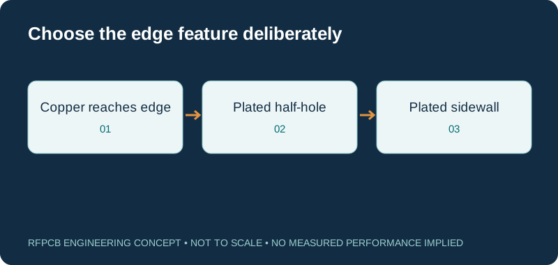
Three edge features that need different instructions
| Feature | What the drawing must identify | What it does not establish |
|---|---|---|
| Copper to board edge | A copper region intentionally reaching the profile | A plated vertical sidewall or controlled contact finish |
| Castellated plated hole | Hole center relative to profile, pads and retained barrel | Universal hole size, remaining copper or solder-joint acceptance |
| Plated sidewall | Required plated segments and connection to designated copper | An uninterrupted plated perimeter without support review |
| Nominal radial ring | Concentric pad diameter and hole diameter on one basis | Tooling compensation, registration allowance or finished acceptance |
| Assembled module joint | Matching motherboard land, paste and assembly requirements | An RF or mechanical result from bare-board inspection alone |
Nominal annular ring calculator
Nominal radial ring = (pad diameter − finished hole diameter)/2. The arithmetic is before registration, routing, etch and plating allowances. A castellation cut through the hole needs additional edge geometry review; this tool does not calculate remaining copper after manufacturing or qualify a design.
Distinguish exposed copper from a plated sidewall
Copper that reaches a routed outline can be visible at the edge without forming the vertical coating needed for a deliberate sidewall connection. A castellation instead uses a partly retained plated hole. These features may sit next to each other in a design, but a manufacturing instruction must identify each one separately.
Eurocircuits describes the same distinction in its edge-feature guidance. Its published processing rules apply to its own service, not automatically to RFPCB. For your design, name the required result on the mechanical drawing and connect that note to the copper data. Avoid a broad “plate all edges” instruction when only selected segments have an electrical purpose.
Define the retained hole against the finished outline
A half-hole feature depends on the relationship between the plated hole and the final profile. Place both in a common coordinate system and dimension from stable datums. Include pad geometry on the relevant layers and identify copper that must connect to the feature.
Do not assume that positioning a hole symbol on an outline is sufficient instruction. State whether the diameter is a finished-hole requirement or a nominal design value and keep that interpretation consistent in the drill table. Request review of the proposed routing and plating sequence, particularly where a nearby corner or narrow web constrains access.
Use the annular ring tool as geometry only
The calculator subtracts hole diameter from pad diameter and divides by two. Both inputs are in millimeters and refer to concentric circles using a consistent dimensional basis. A pad diameter of 1.20 mm and hole diameter of 0.80 mm produce a nominal radial ring of 0.20 mm. This is an illustrative drawing calculation, not an RFPCB process limit.
The result excludes tooling and registration allowances, plating effects and the copper removed by profiling. It therefore does not predict the narrowest finished ring or retained castellation copper. The calculator asks for a pad larger than the finished hole and rejects a zero or negative nominal ring as unusable planning input. A positive result still supplies no manufacturing approval.
Coordinate module pads with the assembly interface
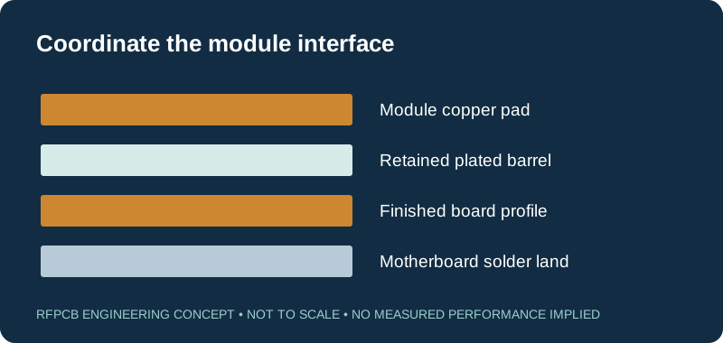
The mother board land pattern, solder paste, module seating and inspection access should be reviewed with the assembly team. A mechanically convenient edge connection can still produce a difficult soldering operation if the mating features are inconsistent. Keep the module outline revision synchronized with its footprint and assembly drawing.
For an RF signal, consider the entire transition from the module trace through the soldered interface into the mother board. Name the accompanying ground connections and reference planes. Nominal hole geometry does not determine transition impedance, and a visible solder fillet does not by itself establish insertion loss. Include an assembled test article when that interface is part of the electrical acceptance requirement.
Plan support and routing before filling the perimeter
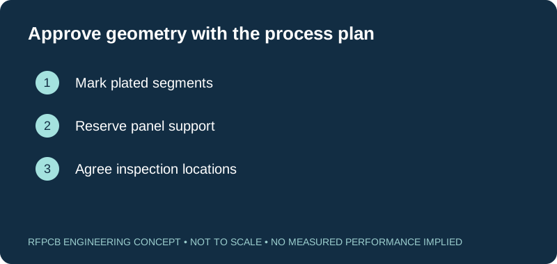
Edge treatments interact with how the board remains supported during processing and separates from the production panel. Identify locations where support features are allowed, together with edges that must remain clear for assembly or enclosure contact. Ask manufacturing to review a heavily occupied perimeter before committing the complete module layout.
Eurocircuits’ published examples show why support and plating sequence deserve attention, but their finish choices and dimensional rules must not be copied into an RFPCB specification as accepted limits. Use the RF DFM checklist to record the proposed panel arrangement, open questions and agreed drawing changes.
Connect plated edges to an intentional grounding design
A plated edge may form part of a grounding or enclosure-contact strategy, but adding metal to the perimeter does not guarantee shielding effectiveness. The electrical result depends on the complete current path, interruptions, connections and mechanical contact conditions. Identify which copper regions connect to the sidewall and which must remain isolated.
For an enclosure interface, dimension the contact region and clarify whether electrical contact is required after assembly. Review fit, compression, coatings and service conditions with the mechanical team. For an RF module, inspect the return path around the edge transition. Treat any claimed improvement in emissions, isolation or loss as a result that requires an appropriate comparison measurement.
Choose finish and inspection scope for the actual joint
Define the finish where soldering or electrical contact occurs and ask whether the proposed construction and process support that requirement. Avoid importing the finish of a familiar connector into a different joint without review.
Specify which visible features require inspection and whether a destructive section is justified. A section can document a chosen location, while a visual check can cover accessible edges; neither automatically represents every hidden region. The test report guide helps connect method, location and sample coverage to the evidence requested with the order.
Quote special processing with comparable assumptions
An edge feature can change preparation, panel utilization, handling and inspection work. Separate those drivers from the cost of the laminate so a quotation comparison reflects the same design. Include prototype quantity, repeat quantity, required inspection records and any assembled validation sample in the inquiry.
The RF PCB cost planner can organize your assumptions, but its demonstration inputs do not price a castellation or plated sidewall. Request a reviewed quote for the actual outline and construction. If a simpler edge arrangement is proposed, compare its effect on assembly and electrical performance before treating the change as an equivalent cost reduction.
Release one consistent edge-feature definition
Provide copper data, drill data, a finished outline and a mechanical drawing that clearly distinguishes plated segments, half-holes and ordinary edges. Include stackup, finish, quantities and the matching module footprint when relevant. Mark unresolved dimensions as questions for review rather than allowing them to become unstated defaults.
RFPCB’s shared-factory capability reference supports discussing edge and half-hole processes; it does not approve every combination of material, thickness and feature size. Record the agreed construction and inspection scope before ordering. For later revisions, highlight changes to the edge interface so the supplier and assembly team can assess whether the earlier process and footprint remain suitable.
Prepare a reviewable engineering request
Check only the requirements you have actually documented. This list records readiness; it does not inspect your files or certify a design. Missing information is useful: identify it explicitly so the engineering review can resolve it before a production release.
These inputs are processed in your browser and are not submitted by this tool. The downloaded summary is a plain-text planning record. Use the secure quote form to send files; request an NDA first if your project requires one.
Manufacturing context
RFPCB and PCBSync share the manufacturing facility shown below. These process photographs illustrate the production environment; they are not evidence that a particular board, material grade or RF performance has been qualified. Request the documentation and inspection scope applicable to your project.



Edge plating and castellation FAQs
Is copper to the edge the same as edge plating?
No. Copper reaching the profile can expose a copper edge without coating the vertical sidewall. Identify the desired plated surface and electrical connection in the drawing.
Does the ring calculator check manufacturing tolerances?
No. It returns only half the nominal pad-minus-hole difference. It includes no tooling, registration or routing allowance and assigns no universal acceptance limit.
Can I put castellations on every side?
Submit the complete outline for review before freezing the design. Support, routing, adjacent features and assembly access must be resolved for that construction; this page makes no blanket perimeter guarantee.
Are Eurocircuits dimensions RFPCB capability limits?
No. Eurocircuits is cited as a primary example of how a manufacturer explains its own process. RFPCB dimensions and finish options require confirmation against the submitted material, stackup and drawing.
Continue your engineering review
Request an edge-feature review with the actual outline
Send the stackup, drill data, mechanical drawing and intended module connection. Mark the plated segments and inspection requirements so the proposed process can be reviewed explicitly.
Sources and engineering scope
- Eurocircuits: castellations as an example of its own process
- Eurocircuits: copper and the board edge; supplier-specific process guidance
- PCBSync: shared-factory edge and half-hole process overview
Manufacturer values apply to the identified grade, test method and construction. Engineering examples on this page are illustrative; they are not measured product results, inventory statements or certification claims. Manufacturer and product names belong to their respective owners. Keep the applicable datasheet revision with your approved manufacturing package.
Ready for a quotation?
Send your requirements for a material, stackup and manufacturing review. Price and schedule are confirmed for your project.