

What Is a PCB Stackup Builder?
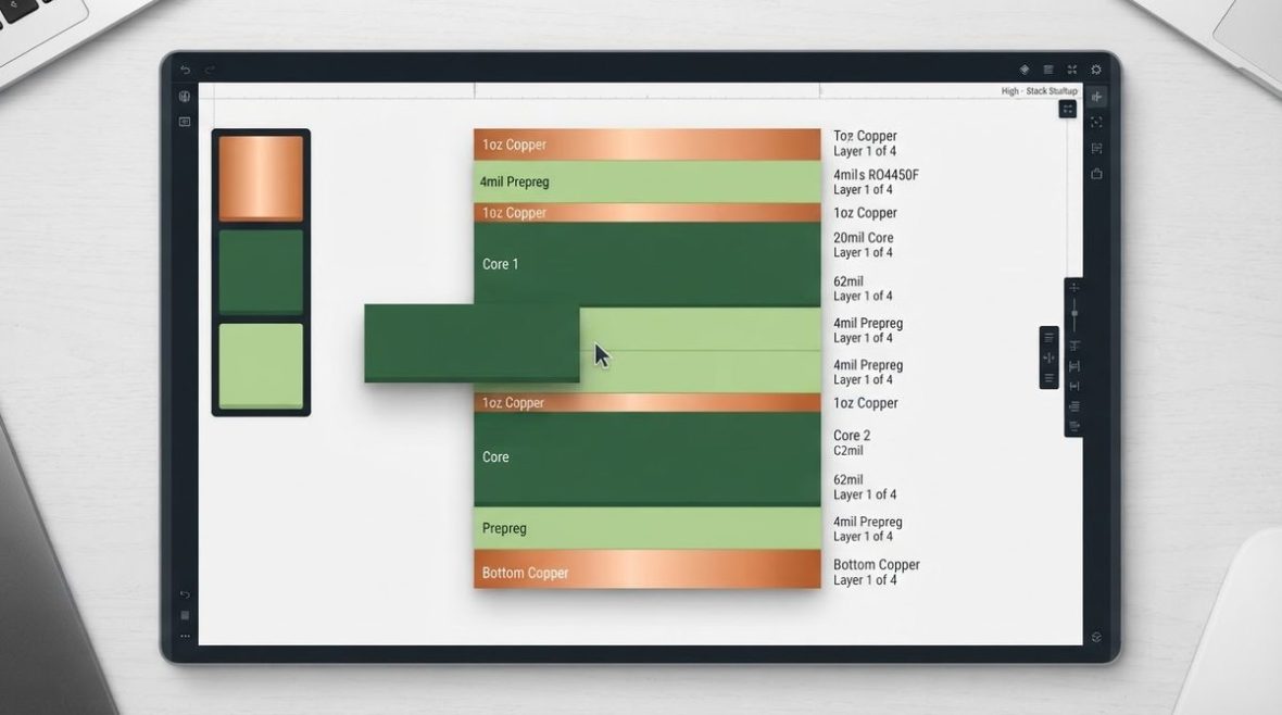
A PCB stackup builder is a visual design tool that lets you drag copper, core, prepreg, and solder-mask layers into a cross-section view and immediately see the resulting impedance, total board thickness, and signal-integrity parameters. Instead of passing spreadsheets back and forth with your fabricator, you define the stackup yourself—choosing materials by Dk, Df, and thickness—and the tool runs field-solver math behind the scenes. For RF and microwave work above 1 GHz, this tight coupling between layer arrangement and impedance calculation is what separates a useful builder from a generic layer editor.
Why RF Engineers Need a Dedicated Stackup Builder
Standard digital-PCB stackup tools assume FR-4 (Dk ≈ 4.2–4.6 at 1 GHz) and focus on layer count and copper weight. RF designs demand more:
- Material-specific Dk/Df: A 50 Ω microstrip on Rogers RO4350B (Dk 3.48, Df 0.0037 at 10 GHz) needs a different trace width than the same impedance on RO3003G2 with Dk 3.00. The builder must carry per-material frequency-dependent data.
- Hybrid stackups: Mixing PTFE RF layers with FR-4 structural layers is routine for cost control, but it changes CTE mismatch and bonding requirements. A builder that flags warpage risk from asymmetric hybrids saves a respin.
- Tight thickness tolerances: At 77 GHz, a 1 mil (25 µm) variation in dielectric height shifts microstrip impedance by roughly 2–3 Ω. The builder should show sensitivity, not just a single nominal number.
- Controlled-impedance structures: Microstrip, stripline, coplanar waveguide with ground (CPWG), and edge-coupled differential pairs each respond differently to the same layer change.
If your design operates above a few gigahertz—or if you are working on 77 GHz automotive radar or 5G mmWave front-ends—a generic stackup planner will leave impedance accuracy on the table.
Core Features of an Effective Stackup Builder
Drag-and-Drop Layer Arrangement
The primary interaction is dragging layers—signal copper, ground plane, core laminate, prepreg sheet, soldermask—into position and reordering them freely. Each layer carries editable properties: copper weight (typically ½ oz, 1 oz, or 2 oz, corresponding to roughly 17.5 µm, 35 µm, or 70 µm finished thickness), dielectric thickness in mils or mm, and material grade. Moving a ground plane one position changes the reference for every adjacent signal layer, so the impedance recalculates instantly.
Live Impedance Calculation
A useful builder does not make you export to a separate field solver. It runs a 2D cross-section model—typically a boundary-element or conformal-mapping engine—on every edit. You should see single-ended impedance (target: usually 50 Ω for RF), differential impedance (often 100 Ω), and insertion loss per unit length (dB/inch at your operating frequency). The board thickness calculator feeds directly from the same layer data, so total thickness and impedance stay synchronized.
Material Library with Frequency-Dependent Data
Dk is not a constant—it drifts with frequency and resin content. A serious builder stores Dk and Df curves (or at least values at multiple test frequencies: 1 GHz, 10 GHz, 77 GHz) for common RF laminates. The table below shows typical values you should expect the library to contain:
| Material | Dk @ 10 GHz | Df @ 10 GHz | Common Use |
|---|---|---|---|
| FR-4 (mid-grade) | 4.30 | 0.020 | Digital / power layers |
| Isola Astra MT77 | 3.00 | 0.0017 | 5G, radar |
| Rogers RO4350B | 3.48 | 0.0037 | General RF, filters |
| Rogers RO3003G2 | 3.00 | 0.0013 | 77 GHz radar, LNAs |
| Panasonic Megtron 7 | 3.37 | 0.0015 | High-speed digital, hybrid RF |
Source values from vendor datasheets; for example, Rogers RO4350B product data confirms Dk 3.48 ± 0.05 at 10 GHz per IPC-TM-650 2.5.5.5.
Symmetry and Warpage Checks
IPC-6012 Class 3 boards require a balanced stackup to control bow and twist below 0.75 %. A good builder flags asymmetry automatically—different copper distribution above and below the midplane, or mismatched CTE in hybrid builds. For deeper background, see our guide on why stackup symmetry matters.
Step-by-Step: Building a 4-Layer Hybrid RF Stackup
Here is a concrete walkthrough for a 4-layer board carrying a 24 GHz patch antenna on top and digital control on inner layers.
- Start with the RF signal layer (L1): Drag a signal-copper layer to the top. Set copper weight to ½ oz (17.5 µm). This will carry the antenna feed and matching network.
- Add the RF dielectric: Place a core layer directly below L1. Select RO4350B, 10 mil (0.254 mm). At 24 GHz with Dk 3.48, a 50 Ω microstrip will be approximately 22 mil (0.56 mm) wide—the builder confirms this live.
- Ground plane (L2): Drag a ground-plane copper layer below the RF core. Set to 1 oz (35 µm). This is the primary RF reference and antenna ground.
- Bonding prepreg: Insert a prepreg layer. For a hybrid, use a low-flow PTFE-compatible prepreg (e.g., Rogers RO4450F, Dk 3.52, 4 mil). This bonds the RF half to the FR-4 half.
- Inner signal layer (L3): Drag a signal-copper layer for digital routing. ½ oz copper.
- FR-4 core: Place a standard mid-Tg FR-4 core, 20 mil (0.508 mm), below L3.
- Bottom ground/power plane (L4): Final copper layer, 1 oz.
- Soldermask top and bottom: Add soldermask layers (typically 0.6–1.0 mil over traces). The builder should account for soldermask Dk (≈ 3.3–3.8) on the RF layer if CPWG structures are used.
Total thickness lands around 47–50 mil (1.19–1.27 mm). The builder should display this sum and compare it against standard board thicknesses (31, 47, 62, 93 mil). If your stackup drifts to 55 mil, the fabricator will likely round to 62 mil by adjusting prepreg—better to catch that now.
Exporting Your Stackup as a Fabrication-Ready PDF
Once the stackup is finalized, export it as a dimensioned cross-section PDF that your fabricator can quote directly. A proper export includes: layer numbering, material call-outs with vendor part numbers, copper weights, dielectric thicknesses with tolerances, impedance targets per layer pair, and any special notes (e.g., “ENIG finish on L1 for wire bonding”). Use the tool below to generate a clean PDF from your finished stackup:
After exporting, open the PDF and verify that the impedance targets match your simulation. A common mistake is forgetting to note the finished-copper thickness (base copper + plating adds roughly 0.5–0.7 mil per side for through-hole plated boards). If your 50 Ω target was calculated for ½ oz base copper but the fabricator plates to 1.2 mil total, impedance drops by 1–2 Ω. Call it out in the notes field before exporting.
Common Pitfalls When Building RF Stackups
- Ignoring etch-back on trace width: The builder calculates impedance for nominal trace width. Fabrication etching narrows traces by 0.5–1.0 mil per side. Enter the post-etch width, not the artwork width, for accurate impedance.
- Using room-temperature Dk at millimeter-wave frequencies: Dk of FR-4 can shift from 4.3 at 1 GHz to 4.1 at 20 GHz. Always check the frequency you entered in the builder.
- Placing two signal layers adjacent without a reference plane: This creates uncontrolled impedance and severe crosstalk. Every signal layer needs a continuous ground or power reference on at least one side.
- Forgetting via transitions in the impedance budget: The stackup builder handles horizontal transmission lines, but a via barrel through multiple layers adds inductance and capacitance. For radar designs, see our radar PCB stackup design guide for via-transition modeling.
Test Your Stackup Knowledge
Think you understand how layer arrangement, material choice, and copper weight interact? The challenge below presents realistic RF stackup scenarios and asks you to identify the correct configuration. It is a quick way to pressure-test your intuition before committing a design to fabrication.
If the challenge reveals a gap—say, you misjudged how moving a ground plane affects stripline impedance—go back to the builder and experiment. Drag the ground plane one position, watch the impedance shift, and internalize the sensitivity. That hands-on loop is faster than any textbook.
From Builder to Fabrication Quote
A finished stackup PDF dramatically speeds quoting. Fabricators can immediately assess whether they stock your chosen laminates, whether the layer count and hybrid bonding are within their process capability, and whether your impedance tolerances (typically ± 10 % for production, ± 5 % for tighter specs per IPC-6012 revision E) are achievable on their equipment. Pair your stackup export with an RF PCB quote configurator to get budgetary pricing before you finalize the design.
Stackup Builder vs. Full Field Solver: When Do You Need Both?
A stackup builder with built-in impedance calculation is accurate enough for initial design and fabrication release of most RF boards through about 40 GHz. Beyond that—especially at 60 GHz and 77 GHz—you benefit from a full-wave 3D field solver (such as Altium’s integrated impedance engine or a standalone tool like Sonnet or HFSS) to capture conductor-surface roughness effects, frequency-dependent Dk dispersion, and via-transition parasitics that a 2D cross-section model cannot resolve. Use the builder to set the stackup, then validate critical nets in the field solver—not the other way around.
FAQ
How many layers does a typical RF stackup builder support?
Most builders handle 2 to 16 layers. For RF front-ends, 2- and 4-layer stackups dominate; digital-RF hybrids commonly reach 6–10 layers.
Can I mix Rogers and FR-4 in the same stackup?
Yes—hybrid stackups are standard practice. Use a compatible bonding prepreg (e.g., Rogers RO4450F or Isola 185HR) between the PTFE/ceramic and FR-4 sections, and keep the stackup symmetric to control warpage.
What impedance tolerance should I specify?
± 10 % is the industry default for controlled impedance per IPC-6012. Tighter tolerances (± 7 % or ± 5 %) are available but increase cost because they require tighter dielectric-thickness and etch control.
Does soldermask affect RF impedance?
Yes. Soldermask (Dk ≈ 3.3–3.8) sits directly on microstrip and CPWG traces, lowering impedance by 2–5 Ω depending on thickness. Either model it in the builder or specify soldermask keep-out over critical RF traces.
How do I share my stackup with the fabricator?
Export a dimensioned cross-section PDF from the builder, including material part numbers, copper weights, impedance targets, and surface-finish requirements. This replaces ambiguous text descriptions and reduces quoting errors.
Ready for a quotation?
Send your requirements for a material, stackup and manufacturing review. Price and schedule are confirmed for your project.