

What Is PCB Reverse Engineering?
PCB reverse engineering is the process of recovering a board’s design data—schematic, netlist, stackup, and layout—from a physical sample when original source files are unavailable. For RF and microwave boards the task is harder than for digital designs: trace geometry controls impedance, dielectric identity determines propagation velocity, and even a 0.5 mil (0.0127 mm) error in copper width can shift a filter’s center frequency by tens of megahertz. The goal is not just connectivity; it is a dimensionally faithful reconstruction of the electromagnetic design.
Common reasons engineers undertake this work include legacy product sustainment, second-source qualification, failure analysis on boards whose OEM has disappeared, and competitive benchmarking. In every case the quality of the recovered data depends on disciplined measurement and an understanding of RF-specific materials and processes.
When Is Reverse Engineering Necessary?
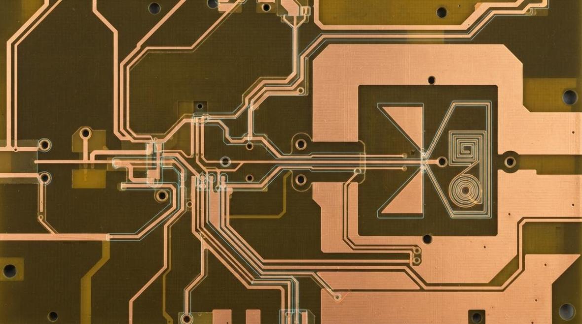
- End-of-life redesign. The original fabricator or laminate is discontinued; you need the stackup and impedance targets to qualify a dual-source equivalent.
- Failure analysis. A field return shows delamination or impedance drift, and no Gerber data exists to compare against.
- Competitive teardown. Understanding a competitor’s material choices and layer count informs your own cost-performance trade-offs.
- IP recovery. A design house closed or a contract ended without a proper data package handoff.
Step-by-Step Reverse Engineering Workflow
Step 1 — Non-Destructive Inspection
Start with what you can learn without cutting the board. High-resolution optical scanning (at least 2400 DPI) captures top and bottom copper artwork. X-ray imaging reveals internal via structures, buried components, and layer-to-layer registration. A time-domain reflectometer (TDR) probe on accessible traces gives a first-pass impedance profile and flags discontinuities such as stubs or via transitions.
Step 2 — Cross-Section and Material Identification
Microsectioning is the single most informative destructive step. A polished cross-section, viewed at 200–500× magnification, reveals:
- Total layer count and copper weights (commonly ½ oz, 1 oz, or 2 oz on RF layers).
- Dielectric thickness between each pair of copper planes, typically measured in mils (1 mil = 0.0254 mm).
- Material type—PTFE-based laminates like Rogers RO4350B (Dk 3.48 ± 0.05) look visually different from woven-glass FR-4 (Dk ≈ 4.2–4.5) under polarized light. Ceramic-filled hydrocarbon materials such as Rogers RO3003G2 have a distinctive granular fill pattern.
- Bonding layers—prepreg versus bond-ply versus thermoplastic adhesive film.
For hybrid stackups that mix RF laminates with FR-4, cross-section analysis is the only reliable way to determine which layers use which material. Understanding the dielectric constant of each layer is essential before any impedance reconstruction can begin.
Step 3 — Layer-by-Layer Imaging
Each copper layer is photographed or scanned after controlled chemical stripping or careful mechanical delamination. For dense boards, progressive milling on a CNC micro-mill exposes one layer at a time. The images are then vectorized into DXF or Gerber format using dedicated reverse-engineering software (tools from vendors such as Altium support bitmap-to-vector conversion with pad and trace recognition).
RF-specific pitfall: microstrip lines on high-frequency laminates often have trapezoidal etch profiles rather than rectangular ones. The effective width at the dielectric interface may be 1–2 mil narrower than the width measured at the top of the copper. Ignoring this undercuts impedance accuracy by 2–5 Ω on a 50 Ω line.
Step 4 — Netlist Extraction
With all layers vectorized and registered, software traces connectivity through vias and pads to generate a netlist. Component footprints are matched against standard packages, and part values are read from markings or confirmed with an LCR meter. For RF passives—especially bare-die MMIC amplifiers, couplers, and filters—package identification can require cross-referencing die size and bond-pad layout against known product families.
Step 5 — Impedance and EM Verification
The recovered stackup and trace dimensions are fed into a 2D field solver to predict characteristic impedance. Compare the calculated values against TDR measurements taken in Step 1. Agreement within ±2 Ω on a 50 Ω line confirms the material identification and geometry are correct. Larger discrepancies usually mean the Dk assumed for a layer is wrong or the dielectric thickness was mis-measured.
For critical RF structures—coupled-line filters, Wilkinson dividers, branch-line couplers—run a 2.5D or 3D electromagnetic simulation on the recovered geometry and compare S-parameters against network-analyzer measurements of the original board.
Recovering the Stackup: The Hardest Part for RF Boards
On a digital board, getting the layer count and approximate thicknesses is usually enough. On an RF board the stackup is the design. A 77 GHz automotive radar front-end built on RO3003 with 5 mil core requires the dielectric thickness to be controlled to ±0.5 mil; a 10 % thickness error shifts the quarter-wave stub length enough to move the passband edge by several hundred megahertz.
Key parameters to recover and verify:
| Parameter | Measurement Method | Typical RF Tolerance |
|---|---|---|
| Layer count | X-ray, cross-section | Exact |
| Dielectric thickness | Microsection + calibrated reticle | ±0.5 mil |
| Copper weight | Microsection copper height | ±0.1 mil |
| Dk at operating frequency | Material ID + datasheet lookup | ±0.02–0.05 |
| Trace width (effective) | Optical + etch-factor correction | ±0.3 mil |
| Surface finish | Visual / XRF | ENIG, ENEPIG, immersion silver, etc. |
Use the interactive stackup challenge below to test your ability to match recovered parameters against known impedance targets. Enter dielectric thickness, Dk, and copper weight, then see whether the resulting impedance hits the 50 Ω mark.
If your result lands between 48 and 52 Ω on a microstrip geometry with a 10 mil RO4350B core and 1 oz copper, your recovered dimensions are in the right ballpark. A result outside that window suggests the Dk or dielectric thickness needs re-examination—go back to the cross-section and re-measure with a calibrated stage micrometer.
Documenting and Exporting the Recovered Stackup
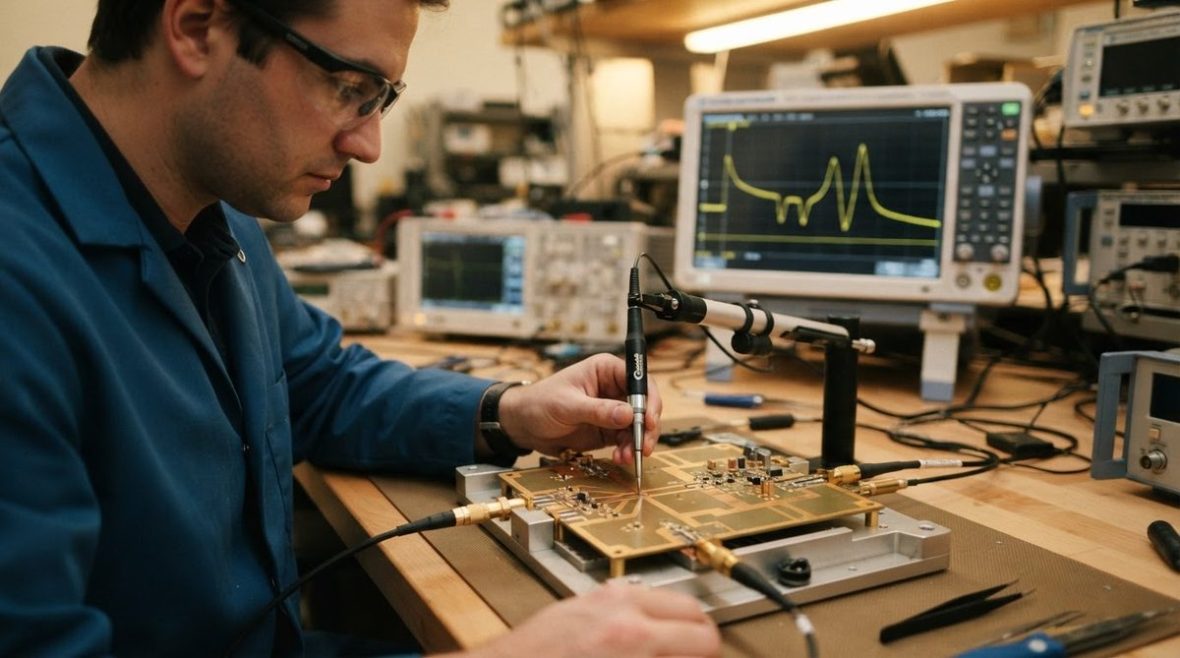
Once the stackup is validated, it needs to be captured in a format that a fabricator can quote and build from. A proper stackup document includes layer sequence, material call-outs with grade and vendor, copper weights, finished dielectric thicknesses, impedance targets, and any special notes on bonding sequence for hybrid Rogers-plus-FR-4 builds.
Export your recovered stackup to a shareable PDF using the tool below. This packages layer data, material grades, and impedance notes into a fabrication-ready drawing.
A clean PDF stackup drawing eliminates ambiguity when sending the recovered design out for quotation. Include tolerances on every dimension—fabricators need them to select the right press cycle and prepreg combination. You can cross-reference your build against proven configurations in our RF PCB stackup library to validate that the recovered structure is manufacturable.
Legal and Ethical Considerations
Reverse engineering a PCB you own for repair, interoperability, or failure analysis is generally lawful in most jurisdictions, but reproducing a patented circuit for commercial sale is not. Key points:
- The physical board itself is not protected by copyright; the schematic and layout as creative works may be, depending on jurisdiction.
- Utility patents may cover specific circuit topologies, matching networks, or antenna structures regardless of how the data was obtained.
- Trade-secret claims can arise if the board was obtained through improper means.
- When in doubt, consult IP counsel before moving from analysis to production.
The companion article on reverse engineering RF PCBs without source files discusses additional practical and legal nuances specific to high-frequency designs.
Common Pitfalls in RF PCB Reverse Engineering
- Assuming FR-4 everywhere. Mixed-dielectric boards are common above 2 GHz. Mis-identifying a PTFE layer as FR-4 introduces a Dk error of 1.0 or more, making every impedance calculation wrong.
- Ignoring etch factor. High-frequency laminates etch differently from FR-4. Always measure trace width at the copper-dielectric interface, not just the top surface.
- Missing embedded passives. Some RF boards use embedded capacitors (thin dielectric between power planes) or resistive foil; these are invisible in a top-down scan.
- Neglecting surface finish effects. At millimeter-wave frequencies, skin-depth losses in ENIG nickel underplate are measurably higher than in bare copper or immersion silver. Record the finish so simulations use the right conductivity.
- Poor via modeling. Back-drilled or laser-drilled microvias behave differently from through-hole vias. A via stub as short as 10 mil creates a resonant notch near 30 GHz per IEEE studies on via-stub effects.
Frequently Asked Questions
How long does PCB reverse engineering take?
A simple 4-layer FR-4 board can be fully recovered in 3–5 working days. A 10-layer hybrid RF stackup with blind vias and MMIC die typically requires 2–4 weeks, including cross-sectioning, EM verification, and documentation.
Can you reverse engineer a PCB from photos alone?
Top and bottom photos recover outer-layer artwork and component placement, but internal layers, dielectric materials, and via structures require X-ray or physical cross-sectioning. Photos alone are insufficient for any board with more than two layers.
What accuracy can be expected on impedance recovery?
With proper cross-sectioning and material identification, recovered impedance values typically match TDR measurements within ±1.5 Ω on 50 Ω structures. The main error sources are Dk uncertainty and etch-profile approximation.
Is reverse engineering the same as cloning?
No. Reverse engineering recovers design data for analysis, repair, or re-design. Cloning implies producing an identical copy for sale, which raises patent and trade-secret issues that reverse engineering for internal use does not.
What software is used for PCB reverse engineering?
Common tools include Altium Designer (bitmap-to-PCB import), Quadcept RE, and dedicated packages from EasyEDA and PCBI. For RF boards, a 2D field solver (e.g., Polar Si9000) and a full-wave EM simulator (Ansys HFSS, Sonnet) are essential complements.
Ready for a quotation?
Send your requirements for a material, stackup and manufacturing review. Price and schedule are confirmed for your project.