
High-Dk RF materials · Compact circuit planning
Rogers RO3006 and RO3010 PCBs use ceramic-filled PTFE laminates with relatively high dielectric constants. They are candidates for compact RF structures, but size reduction must be balanced against geometry sensitivity, temperature behavior and a qualified fabrication construction.
RO3006 and RO3010 offer different high-Dk starting points for RF design. A higher dielectric constant can shorten an ideal guided wavelength, but it does not automatically improve bandwidth, efficiency or manufacturing tolerance. Use an appropriate material model and validate the complete circuit.
RO3006 and RO3010 manufacturer reference values
| Reference property | RO3006 | RO3010 |
|---|---|---|
| Material family | Ceramic-filled PTFE | Ceramic-filled PTFE |
| Typical process Dk | 6.15 ± 0.15 | 10.20 ± 0.30 |
| Published design Dk | 6.4 | 11.2 |
| Typical Df at 10 GHz | 0.0020 | 0.0022 |
| Typical thermal coefficient of Dk | −262 ppm/°C | −395 ppm/°C |
| Use of these figures | Modeling references, not board acceptance limits | Modeling references, not board acceptance limits |
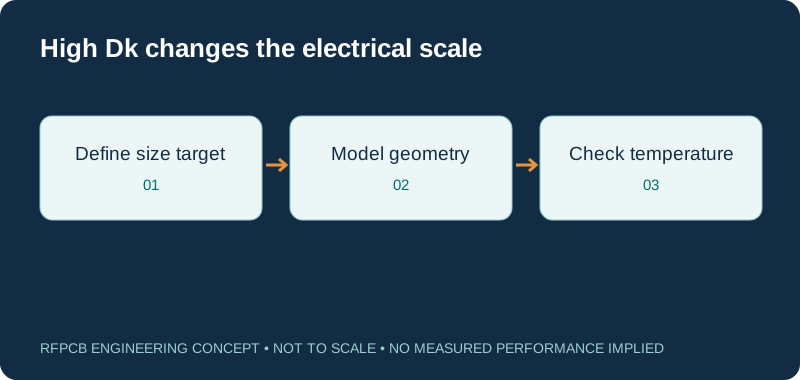
Guided wavelength and size explorer
λg = c / (f × √εeff), with c = 299.792458 mm·GHz. Use the effective value of your actual geometry. Quarter wavelength excludes fringing, loading, dispersion, coupling and end corrections. It is not production-ready artwork.
What is a RO3010 or RO3006 PCB?
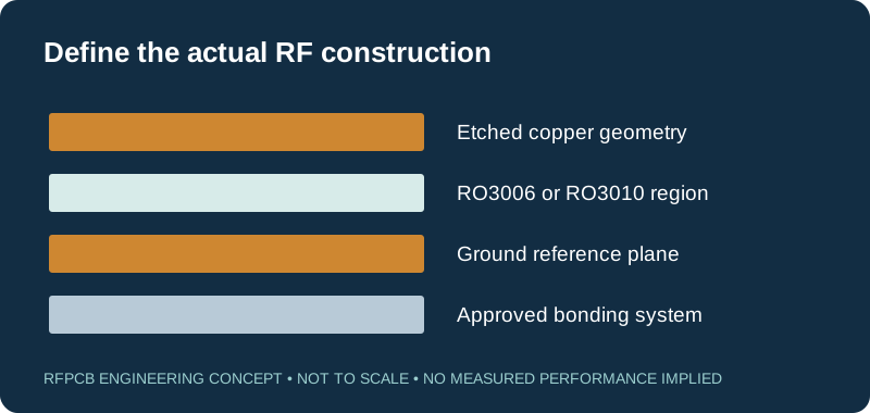
The material name identifies a laminate used in one or more dielectric regions of the board. It does not define the number of copper layers, final thickness, foil profile, bonding material or surface finish. A complete manufacturing specification must identify those details independently.
A simple two-layer construction and a hybrid multilayer board can both use one of these materials, yet have very different field distributions and processing requirements. Ask for a layer-by-layer stackup and use it as the shared reference between the RF designer, mechanical engineer, purchasing team and fabricator.
Understand the miniaturization opportunity
Increasing effective permittivity reduces the guided wavelength in an ideal transmission structure. That can make a compact resonant path possible, but the physical layout still depends on the field distribution, loading and coupling. A size estimate based on bulk Dk alone is not enough to generate final artwork.
The wavelength explorer above accepts effective permittivity so you can see the relationship directly. Use a value from an appropriate geometry model and compare one assumption at a time. The calculated quarter wavelength excludes fringing and end corrections, so it is a starting scale rather than a tuned dimension.
High-Dk designs can be sensitive to small dimensional changes
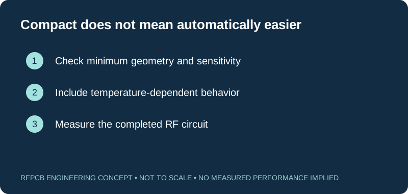
A compact circuit can place critical behavior into shorter paths and smaller gaps. Etch variation, copper thickness, registration and dielectric thickness may become important parts of the tolerance budget. Review both the nominal design and plausible manufacturing variation rather than optimizing only one ideal geometry.
Identify which dimensions need explicit inspection and how their acceptance limits relate to RF performance. Use the controlled-impedance guide for routed lines, and agree a separate measurement plan for resonant or coupled features. A generic impedance report does not validate every circuit dimension.
Pay attention to temperature-dependent dielectric behavior
The published thermal coefficients in the table are a reminder to model the operating environment, not to assume every ceramic-filled PTFE grade behaves identically. Do not transfer the temperature characteristics of another RO3000 product to RO3006 or RO3010. Consult the relevant manufacturer data and its stated conditions.
If resonance or phase must remain controlled across temperature, define the operating range and acceptance method. The finished response also depends on geometry, copper and mechanical attachment. Room-temperature agreement between a model and a prototype does not by itself establish behavior over the full product environment.
Keep the design model distinct from procurement tolerances
A procurement reference and an RF modeling parameter serve different purposes. Preserve the source, test convention and revision of the values used in a simulation. Effective permittivity then follows from the structure being modeled, including how fields occupy the dielectric and surrounding region.
For a sensitive circuit, correlate the chosen model with a representative test structure or prototype. If the model changes after measurement, keep that update in the design record. Avoid leaving one value in the simulation, another on the stackup and a third in the purchasing email without explaining their roles.
Review PTFE-compatible fabrication and bonding
The process review should cover handling, hole preparation, metallization, dimensional compensation and the proposed bonding system. For multilayer construction, identify the material between every relevant pair of copper layers and the pressed thickness. Do not treat an RF core designation as a complete lamination recipe.
A hybrid stackup can be investigated where only selected regions need the high-Dk material. Compatibility, symmetry and the electrical contribution of bonding layers require confirmation. The approved drawing should be established before narrow controlled routes and mechanical interfaces are finalized.
Choose copper and finish with the RF path in mind
The laminate does not remove conductor loss or the effect of surface processing. State the copper foil requirements, final copper assumptions and the areas covered by solder mask. Connector pads, matching networks and resonators may need different attention from digital support routing.
Use the RF surface-finish guide to discuss assembly, storage and electrical tradeoffs. Specify the selected finish in the quotation request and model sensitive areas consistently. A photograph with gold-colored conductors cannot identify the exact finish stack or prove the laminate grade.
Quote the exact construction and quantities
A useful quotation requires dimensions, accepted-board quantity, layer arrangement, dielectric thickness, copper and finish. Identify any special holes, cavities, edge treatment or test structures. Request confirmation of the exact material configuration and availability for the planned order rather than assuming every thickness is held in stock.
The RF PCB cost model can separate panel allocation, fixed preparation and variable fabrication assumptions. Use the resulting summary to explain a scenario, then obtain a reviewed commercial quotation. Demonstration inputs do not establish the price of RO3006 or RO3010 boards.
Plan a prototype that resolves the selection question
If both grades are candidates, define what would make one preferable: board area, resonance, loss, bandwidth, temperature response or manufacturing tolerance. Keep the test setup and assembly conditions controlled so the comparison is interpretable. Record any tuning or geometry changes made during the trial.
A final release should preserve the selected grade, approved stackup, tuned artwork and acceptance requirements. For broader context, compare the lower-Dk RO3003 option or the filter manufacturing guide. The best choice is the one supported by the relevant evidence.
Prepare a reviewable engineering request
Check only the requirements you have actually documented. This list records readiness; it does not inspect your files or certify a design. Missing information is useful: identify it explicitly so the engineering review can resolve it before a production release.
These inputs are processed in your browser and are not submitted by this tool. The downloaded summary is a plain-text planning record. Use the secure quote form to send files; request an NDA first if your project requires one.
Manufacturing context
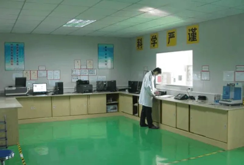
RFPCB and PCBSync share the manufacturing facility shown below. These process photographs illustrate the production environment; they are not evidence that a particular board, material grade or RF performance has been qualified. Request the documentation and inspection scope applicable to your project.


RO3006 and RO3010 PCB FAQs
Does RO3010 automatically make my antenna smaller?
It can change the electrical scale of a structure, but the final antenna also depends on geometry, fields, bandwidth, efficiency and the installed environment. Use an appropriate electromagnetic model and representative measurement rather than a simple bulk-Dk size ratio.
Can RO3006 replace RO3010 without changing artwork?
Do not assume so. Their dielectric references differ, which can alter impedance, electrical length and coupling. A substitution requires a reviewed model and acceptance evidence for the actual construction and circuit.
Are the displayed Dk values the values for every simulation?
No. The table distinguishes manufacturer process and design references. Use the model appropriate to the specified construction and method; derive effective permittivity from geometry when needed. Keep source revisions and correlation evidence with the design.
What thicknesses and delivery times are available?
Availability must be confirmed for the exact grade, thickness, foil and quantity. Send the required stackup and schedule for review. This page does not represent a live stock list or promise a fixed manufacturing lead time.
Continue your engineering review
Request a high-Dk PCB construction review
Send the selected grade, frequency band, critical dimensions and operating-temperature requirements. Include the stackup, quantities and measurement scope for a meaningful quotation.
Sources and engineering scope
Manufacturer values apply to the identified grade, test method and construction. Engineering examples on this page are illustrative; they are not measured product results, inventory statements or certification claims. Rogers product names are trademarks of their owner. Keep the applicable datasheet revision with your approved manufacturing package.
Ready for a quotation?
Send your requirements for a material, stackup and manufacturing review. Price and schedule are confirmed for your project.