
PTFE composites · Material and construction selection
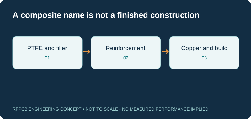
Ceramic-filled PTFE PCB materials combine a fluoropolymer resin with ceramic filler; some grades also contain woven glass reinforcement. Select the exact composite, thickness and copper for your RF path. The category is different from a solid alumina or aluminum-nitride ceramic substrate.
Choose a ceramic-filled PTFE laminate by grade-specific electrical data, reinforcement, foil and processing requirements. RO3000 materials are examples of this composite family; RO3200 materials add woven glass reinforcement. A higher Dk can change electrical dimensions, but neither the filler description nor nominal Dk establishes finished-board loss, thermal performance or manufacturing approval.
Keep the material systems distinct
| Material system | What the description means | Selection consequence |
|---|---|---|
| Ceramic-filled PTFE | PTFE resin with ceramic filler; identify reinforcement separately | Specify exact grade, copper and dielectric thickness |
| Woven-glass ceramic-filled PTFE | PTFE and ceramic with woven-glass reinforcement | Include reinforcement and construction in the model |
| Hydrocarbon/ceramic thermoset | A different polymer system, including RO4360G2 | Do not transfer PTFE processing assumptions |
| Solid ceramic substrate | Ceramic body such as alumina or aluminum nitride | Separate substrate, metallization and assembly review |
| Multilayer RF construction | Core plus bonding layers, copper and plated features | Define every electrically important dielectric region |
| Finished RF PCB | A manufactured circuit with measured geometry | Accept against agreed board and RF requirements |
Guided wavelength and size explorer
λg = c / (f × √εeff), with c = 299.792458 mm·GHz. Use the effective value of your actual geometry. Quarter wavelength excludes fringing, loading, dispersion, coupling and end corrections. It is not production-ready artwork.
Separate ceramic filler from a ceramic substrate
The word ceramic can describe very different circuit materials. In a ceramic-filled PTFE laminate, the filler is part of a polymer composite. A solid alumina substrate uses a ceramic body and a different construction approach. A procurement description such as “ceramic RF board” therefore leaves a fundamental question unresolved. Request the manufacturer and full product name before discussing substitutions, electrical dimensions or processing.
Rogers identifies the RO3000 family as ceramic-filled PTFE in its RO3000 datasheet. The PTFE PCB guide provides the wider resin-family context. Keep the distinction visible in the drawing and quotation so a buyer does not compare unlike substrates under one material label. If an existing design uses a ceramic body, changing to a filled polymer is a new construction evaluation, including attachment, geometry, thermal paths and product qualification.
Record reinforcement as part of the material identity
Ceramic filling and glass reinforcement are separate descriptors. Rogers explicitly distinguishes RO3000 ceramic-filled PTFE from the woven-glass-reinforced RO3200 composites in its processing reference. Do not infer the presence of woven cloth merely because a laminate contains ceramic, and do not assume every PTFE laminate shares the same mechanical response.
For engineering review, identify whether the candidate contains woven glass, another reinforcement or no woven cloth, using the manufacturer's exact description. Retain the material orientation when it affects the released drawing or supplier model. Ask the fabricator to review thin-core handling, registration and the finished outline in the actual layer construction. The objective is a complete bill of materials and a repeatable manufacturing proposal. It is not a general ranking in which reinforcement is always beneficial or an unreinforced laminate is automatically unsuitable.
Use grade-specific dielectric references
An illustrative set of process Dk values shows why a family label is insufficient: the referenced RO3000 sheet lists RO3003 at 3.00 ± 0.04, RO3006 at 6.15 ± 0.15 and RO3010 at 10.2 ± 0.30, using IPC-TM-650 2.5.5.5 at 10 GHz and 23°C. These are different grades with different electrical properties. The values are reference data, not permission to copy a completed layout between them.
Continue to RO3003 PCB or RO3006 and RO3010 PCB for the relevant grade discussion. Record process Dk, design Dk and modeled effective permittivity in separate fields. Preserve the document revision and method beside each entry. Where a product page, older PDF and simulation library disagree, resolve the model with the material supplier before releasing a sensitive design.
Explore electrical size without promising board shrinkage
The guided-wavelength tool uses frequency and effective permittivity to calculate an ideal propagation length. Increasing effective permittivity reduces that wavelength in the model. This is useful when comparing the scale of a resonator, feed section or phase path, provided the selected effective value represents the actual transmission structure. A published bulk-material number is not automatically the correct input for an exposed microstrip.
The tool does not calculate a finished antenna outline or predict a fixed percentage reduction in board area. Connectors, component footprints, clearances and assembly constraints may determine most of the outline. A smaller electrical feature can also become more sensitive to a given dimensional error. Use a consistent field model to review both nominal response and manufacturing tolerances, then decide whether the available physical space actually benefits from the higher-permittivity construction.
Budget loss for the complete signal path
A low dielectric loss tangent addresses one part of a transmission path. Copper texture, conductor dimensions, surface finish, launches, vias and neighboring structures also influence the response. Define the operating band and the permitted end-to-end loss before choosing a material from a table. Identify whether the concern is a long uniform feed, a compact filter or a transition-dominated interconnect.
The RF PCB loss guide helps separate distributed line loss from discrete features. For a proposed material change, compare constructions at the same frequency and with clearly defined measurement planes. If the copper or geometry changes at the same time, describe the result as a construction comparison. Do not attribute every measured improvement to ceramic content or Df. Ask for the model or test evidence that resolves the dominant part of the budget.
Review PTFE processing with the complete hole schedule
A ceramic filler does not make a PTFE composite interchangeable with a conventional thermoset laminate in fabrication. The Rogers RO3000/RO3200 reference calls for PTFE-compatible hole preparation before metal deposition. That is a process-planning distinction; it does not establish which finished hole size, layer count or board thickness a particular factory has qualified.
Supply the proposed stackup, plated and nonplated hole schedule, finished dimensions and any controlled edges. Mark holes that pass through both PTFE and another dielectric system. Ask how the reviewed process addresses hole-wall preparation, bonding and inspection for that construction. Where reliability is critical, define appropriate evidence with the fabricator and product owner. A previous two-layer sample or a photograph of drilling equipment cannot qualify every multilayer version. Keep the approved construction and inspection scope tied to the board revision.
Include bond layers in the electrical and mechanical review
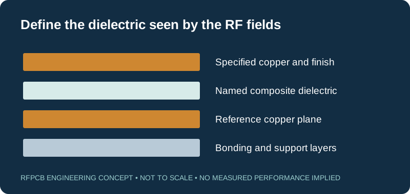
A multilayer board contains dielectric regions beyond the named RF core. The bonding material, its pressed thickness and the copper distribution can change the environment around an internal route or transition. Show each core and bonding layer on the stackup, including the reference planes used by sensitive signals. Avoid hiding an unspecified bonding system under a generic “PTFE multilayer” note.
For a hybrid RF stackup, explain which layers need the selected composite and which layers support control or power functions. Ask for a proposed bonding construction and identify what is provisional. Compare alternatives using the final pressed arrangement, not only nominal incoming-sheet thickness. Review layer symmetry, registration requirements and the path through plated features together. Changing a support region can still matter when a signal transition or thermal path crosses that region.
Treat thermal conductivity as one model input
Ceramic-filled does not mean that every grade is a high-conductivity heat spreader. Thermal behavior belongs to the named material, measurement direction and test conditions. A board-level temperature estimate also needs power dissipation, source area, copper distribution, thermal vias, attachment interfaces and the cooling boundary. Do not infer a safe device temperature from the laminate category.
For a power amplifier, identify where the heat enters the board and how it reaches the enclosure or heat sink. Separate electrical loss heating from device dissipation when building the model. If a substrate change is proposed to improve temperature, keep the rest of the comparison controlled and measure the relevant locations under a defined load. Record ambient conditions, mounting pressure where applicable and operating duty. That evidence is more useful than comparing conductivity numbers without the physical route through which heat must travel.
Choose coupons that represent the sensitive feature
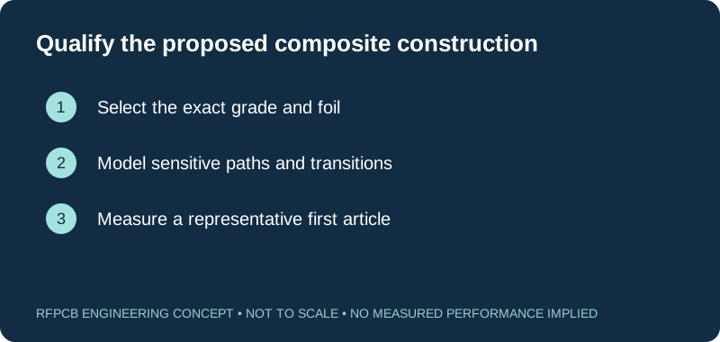
Before ordering a prototype, decide which uncertainty the test should reduce. A straight transmission line can help characterize distributed behavior, but it may not represent a tightly coupled filter, a connector launch or an antenna mounted near metal. Select the actual structure or a justified representative coupon, and document the relationship to the production design.
Agree the frequency sweep, reference planes, calibration approach and acceptance limits before fabrication. Preserve raw measurement data, processed results and the measured geometry where relevant. If the build uses several material grades, label the samples clearly enough to prevent a data mix-up. Record the exact copper, finish and bonding system with the results. A useful qualification record connects the material identity to a defined board revision and measurement setup, making later changes assessable without relying on a remembered material nickname.
Request a construction-specific manufacturing proposal
Send the design files, target quantity, exact composite grade and proposed stackup through the project quote form. State the operating band, critical RF paths and the evidence expected with the boards. If material selection is still open, list candidate grades and the requirement driving the comparison. Mark which dimensions can change and which mechanical interfaces are fixed.
Separate confirmed quotations from planning assumptions when comparing costs. Material allocation, fabrication preparation, inspection and qualification can affect the delivered result differently at prototype and production quantities. This guide does not establish current stock, an approved manufacturing process for every grade or a fixed delivery promise. Ask for a written proposal identifying material sourcing, the reviewed construction and open engineering items. Retain that proposal with the accepted drawing so a later availability-driven substitution triggers the right technical review.
Prepare a reviewable engineering request
Check only the requirements you have actually documented. This list records readiness; it does not inspect your files or certify a design. Missing information is useful: identify it explicitly so the engineering review can resolve it before a production release.
These inputs are processed in your browser and are not submitted by this tool. The downloaded summary is a plain-text planning record. Use the secure quote form to send files; request an NDA first if your project requires one.
Manufacturing context
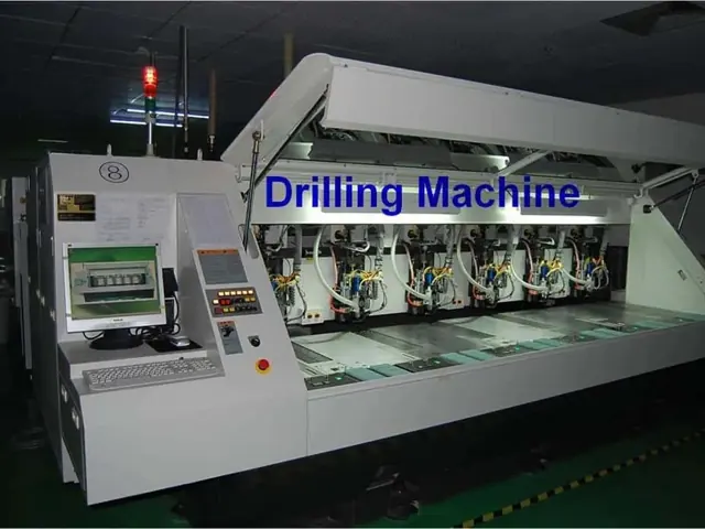
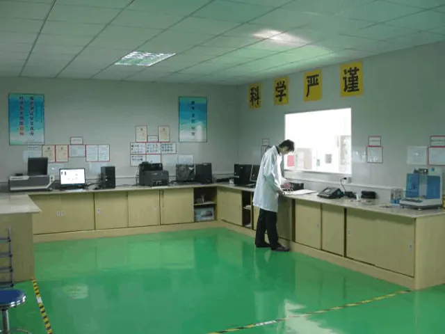
RFPCB and PCBSync share the manufacturing facility shown below. These process photographs illustrate the production environment; they are not evidence that a particular board, material grade or RF performance has been qualified. Request the documentation and inspection scope applicable to your project.

Ceramic-filled PTFE PCB questions
Is ceramic-filled PTFE the same as an alumina PCB?
No. It is a polymer composite containing ceramic filler. An alumina substrate has a ceramic body and requires its own metallization, attachment and construction review. Use an exact material designation instead of the ambiguous phrase ceramic PCB.
Does every ceramic-filled PTFE laminate contain woven glass?
No. Reinforcement is grade-specific. Rogers distinguishes RO3000 ceramic-filled PTFE products from woven-glass-reinforced RO3200 materials. Confirm the exact manufacturer description and construction rather than inferring reinforcement from the filler.
Does higher Dk always make the complete PCB smaller?
Higher modeled effective permittivity reduces an ideal guided wavelength. The final board may still be controlled by components, connectors, clearances and mechanical interfaces. Field distribution, tolerance sensitivity and coupling require a circuit-level review.
Can the wavelength tool produce fabrication-ready geometry?
No. It illustrates electrical scale in a simplified propagation model. It excludes fringing, loading, dispersion, coupling and end corrections. Use appropriate electromagnetic analysis and a representative manufactured test structure for critical artwork.
Continue your engineering review
Request a ceramic-filled PTFE construction review
Provide the exact material candidate, stackup and RF requirements. Request a documented proposal that connects sourcing and fabrication scope to the evidence needed for your design.
Sources and engineering scope
- Rogers RO3000 series datasheet: composite identity and method-specific electrical properties
- Rogers RO3000/RO3200 quick-reference processing guide
- Rogers: composition and reinforcement in low-loss RF microwave laminates
- Rogers: circuit materials and high-frequency PCB losses
Manufacturer values apply to the identified grade, test method and construction. Engineering examples on this page are illustrative; they are not measured product results, inventory statements or certification claims. Manufacturer and product names belong to their respective owners. Keep the applicable datasheet revision with your approved manufacturing package.
Ready for a quotation?
Send your requirements for a material, stackup and manufacturing review. Price and schedule are confirmed for your project.