
Connected devices · Antenna and link planning
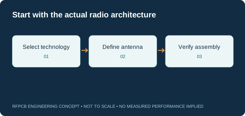
RFID, IoT and LoRa PCB design covers several different radio architectures. Define the actual technology, operating band, antenna and product environment before choosing the board construction. The link-budget tool organizes an assumed radio path for engineering discussion.
Build the PCB around the selected radio and antenna reference, then verify the assembled product. HF RFID, UHF RFID and LoRa are different design cases. A positive calculated link margin is a planning result; it does not establish range, packet reliability or authorization to operate in a region.
Different wireless applications need different PCB questions
| Application | Primary design question | Information to freeze |
|---|---|---|
| HF RFID / NFC | How does the coil interact with the reader and nearby materials? | Coil geometry, tuning network and intended assembly |
| UHF RFID | Is this a reader path or a passive tag interface? | Selected band, chip interface and antenna model |
| LoRa sensor node | Which radio mode, antenna and power conditions apply? | Radio settings, regional variant and RF layout |
| LoRaWAN device | How will the radio join and operate in the intended network? | Protocol configuration plus radio hardware requirements |
| General IoT radio | What environment surrounds the antenna in use? | Enclosure, ground area, battery and mounting |
| Production test | Which accessible measurements identify assembly faults? | Test connection, settings, limits and fixture revision |
Radio link budget planner
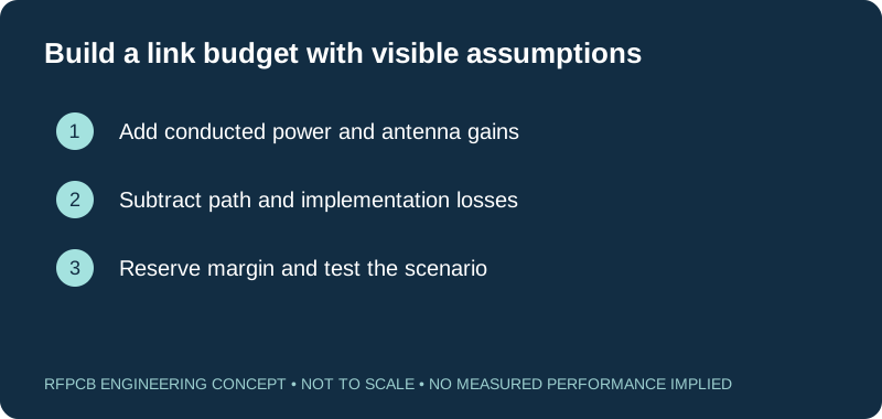
Received power = conducted power + antenna gains − path loss − other losses. Margin is received power minus receiver sensitivity; remaining margin also subtracts the selected fade reserve. Do not enter EIRP as conducted power and add transmit antenna gain again. Sensitivity must match bandwidth, modulation and packet-error criterion. This does not determine lawful radiated power or usable range.
Separate HF RFID, UHF RFID and LoRa requirements
HF RFID and NFC commonly use 13.56 MHz interfaces; UHF RFID belongs to a different frequency family and uses different antenna and chip arrangements. NXP distinguishes these technology families in its RFID and NFC portfolio. Do not transfer a coil layout or matching assumption from one family to the other.
For RFID, also identify reader versus tag and active versus passive architecture. A passive tag needs an appropriate chip-powering and response analysis. The one-way receiver link calculator on this page is not a passive-tag read-range model and does not calculate the backscatter return path.
Distinguish LoRa modulation from LoRaWAN networking
Semtech identifies LoRa as the physical radio modulation and LoRaWAN as a networking protocol in its LoRa and LoRaWAN guide. A board with a LoRa-capable transceiver does not by itself define network behavior. Record the intended protocol, firmware configuration and counterpart device or gateway.
Treat labels such as 868 MHz and 915 MHz as incomplete product specifications. Identify the target market and have the responsible team establish permitted frequencies, power, channel behavior and conformity requirements. This page provides no worldwide license-free claim. Semiconductor tuning range and a regional reference design are not operating authorization.
Start from a reference that matches the selected radio
Choose the correct radio part, band and RF output configuration before using a reference layout. Semtech publishes separate SX1262 reference designs and application documents on its device resource page. Preserve the identity of the selected reference with the schematic and explain deliberate departures from it.
Highlight changed component packages, RF routing, ground geometry and antenna connection on a comparison drawing. Review each difference before fabrication. Retaining component values while rearranging them does not establish RF equivalence. Record tuning changes in the final BOM.
Reserve antenna geometry before the mechanical design closes
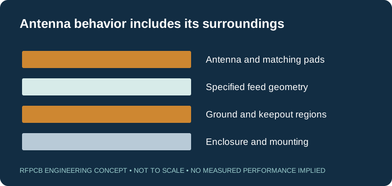
An antenna uses space that other product teams may also want: an edge, a ground region or separation from a battery and mounting hardware. Include that space in the mechanical drawing early. Define which copper layers, components and enclosure parts may occupy each region, using the chosen antenna supplier’s requirements.
TI’s antenna impedance and matching report illustrates detuning from a plastic case and nearby loading. Its examples support measuring the intended assembly rather than copying their numerical matching values. Keep the enclosure revision and measurement setup with the antenna results so a later mechanical change can be evaluated against the same baseline.
Choose the laminate for the actual feed and board size
A compact sensor node is not automatically improved by using an RF laminate throughout its entire stackup. Identify the relevant trace lengths, impedance requirements, dimensional sensitivity and fabrication constraints first. Discuss a standard or RF construction using the material selection guide, with the actual operating band and layout available.
The impedance calculator can help organize a preliminary feed geometry. Confirm that geometry against the proposed construction before release. An antenna clearance is not the same as a transmission-line reference: document where ground is required and where the chosen antenna design calls for a keepout.
Read the link-budget outputs without hiding assumptions
The calculator uses received power = transmit power + transmit antenna gain + receive antenna gain − total path loss − miscellaneous losses. Net margin = received power − receiver sensitivity − reserved fade margin. Power is entered in dBm, gains in dBi and losses or margins in dB.
Enter conducted transmit power, not an EIRP value that already includes antenna gain. Keep propagation loss separate from cable, connector and implementation losses, and avoid counting any loss twice. Use receiver sensitivity for the selected operating mode. The calculation subtracts your supplied values; it does not derive path loss from distance or predict the installation environment.
Test a conservative scenario as well as the nominal one
A positive margin says that the entered received power exceeds the entered threshold after your reserve. It does not show how frequently the path will experience a worse condition. Create scenarios for the antenna orientation, mounting position and obstruction conditions relevant to the product, using justified inputs instead of choosing values to reach a desired result.
An additional 3 dB of miscellaneous loss reduces calculated net margin by 3 dB. This helps compare a cable or matching change, but cannot establish packet delivery under interference or changing conditions. Preserve the assumptions beside any reported margin.
Separate antenna matching, filtering and production checks
Matching and unwanted-emission control answer different questions. Review the complete RF path, including any switch or filter, with the filter and duplexer PCB guide. A well-matched antenna does not by itself demonstrate an acceptable transmitted spectrum or receiver behavior.
For production planning, identify an accessible test point and specify the board state, firmware settings and fixture connection. Decide which measurements belong to assembly screening and which require a more complete product test. Include reference-plane information when cables or connectors are part of the result. Do not label a continuity-tested bare board as a verified radio.
Release the RF variant and its evidence together
A repeat order should identify the antenna geometry, board revision, matching BOM and intended regional variant. A late change to the enclosure, battery holder or feed connector should trigger review of the affected evidence. The RF PCB DFM checklist helps collect the manufacturing portion of that package.
Compare prototype and production scope using the RF PCB cost calculator. Include tuning samples and test fixture work. Send controlled files and open questions through the quote form for review.
Prepare a reviewable engineering request
Check only the requirements you have actually documented. This list records readiness; it does not inspect your files or certify a design. Missing information is useful: identify it explicitly so the engineering review can resolve it before a production release.
These inputs are processed in your browser and are not submitted by this tool. The downloaded summary is a plain-text planning record. Use the secure quote form to send files; request an NDA first if your project requires one.
Manufacturing context
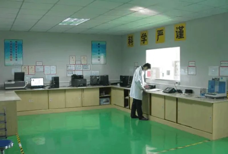
RFPCB and PCBSync share the manufacturing facility shown below. These process photographs illustrate the production environment; they are not evidence that a particular board, material grade or RF performance has been qualified. Request the documentation and inspection scope applicable to your project.


RFID, IoT and LoRa PCB FAQs
Is LoRa the same as LoRaWAN?
No. LoRa is the physical radio modulation; LoRaWAN defines networking behavior above the radio layer. Specify the intended hardware, firmware and network together. A LoRa-capable PCB is not proof that a finished product meets its network requirements.
Can the link-budget calculator predict LoRa range?
No. It evaluates supplied power, gain, loss, sensitivity and fade-margin values. It does not calculate terrain, obstruction, interference or probability of successful packets. A range claim needs a defined environment, configuration and supporting measurements.
Can I use this calculator for an HF RFID coil or passive UHF tag?
It is not a coil-coupling or passive-tag read-range model. HF operation needs the relevant coupling and tuning analysis. Passive UHF RFID also involves tag activation and a return path that this one-way receiver calculation does not represent.
Can one 868 or 915 MHz board be shipped everywhere?
Do not assume so. The product team must review the intended market, frequency plan, output settings, antenna and applicable requirements. A frequency printed on a module or reference design is not a worldwide operating permission.
Continue your engineering review
Request a board review for your wireless product
Send the selected radio, frequency variant, antenna layout and enclosure context. Include the fabrication files, quantities and measurements required for your prototype plan.
Sources and engineering scope
- Texas Instruments SWRA726: antenna impedance measurement and matching
- Semtech AN1200.86: LoRa and LoRaWAN
- Semtech SX1262: application documents and regional reference designs
- NXP: RFID and NFC technology families
Manufacturer values apply to the identified grade, test method and construction. Engineering examples on this page are illustrative; they are not measured product results, inventory statements or certification claims. Manufacturer and product names belong to their respective owners. Keep the applicable datasheet revision with your approved manufacturing package.
Ready for a quotation?
Send your requirements for a material, stackup and manufacturing review. Price and schedule are confirmed for your project.