
Engineering release · Interactive checklist
RF PCB DFM connects the electrical design to a manufacturing package that can be reviewed and reproduced. Work through the checklist, record unresolved questions and download a summary before requesting fabrication or assembly.
A DFM checklist is a preparation aid, not an automated Gerber inspection. It should expose missing material definitions, ambiguous impedance requirements, unreviewed via structures and unclear acceptance criteria. A checked box records your assessment; only a project-specific engineering review can resolve manufacturability.
RF DFM review: input, risk and release evidence
| Review area | Common gap | Information to release |
|---|---|---|
| Files and revision | Gerber, drill and drawing revisions disagree | One controlled package and change record |
| Material and stackup | Brand name without construction | Exact dielectrics, foil, bonding and thicknesses |
| RF routing | Impedance number without reference plane | Controlled nets, layers, model and tolerance |
| Vias and transitions | Hole diameter without layer pair or fill | Via structure, landing geometry and process sequence |
| Finish and assembly | RF-sensitive regions not identified | Finish, mask, component and assembly notes |
| Acceptance | “RF tested” without a method | Article, fixture, reference planes, limits and reports |
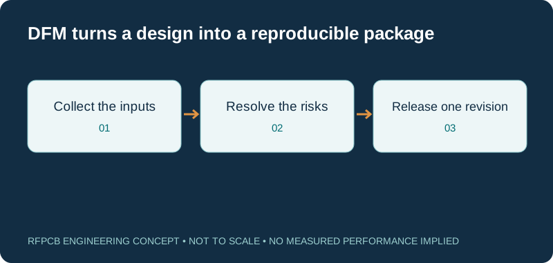
Begin with one consistent release package
Provide fabrication data, drill files, outline and drawings from the same design revision. Include a readme that identifies the revision, intended quantity and whether the package is for quotation, prototype manufacture or production release. Avoid placing several unexplained alternatives in one archive.
Check that units and coordinate origins are consistent and that the board outline is unambiguous. Identify nonplated holes, slots and cutouts. If the supplier proposes a change, record it against the package revision and keep approval separate from an informal discussion about a possible option.
Define the laminate beyond its brand name
Specify the manufacturer and exact grade, dielectric thickness, copper requirements and permitted alternatives. For a hybrid construction, name the material in each relevant region rather than labeling the entire board as Rogers or PTFE. Include bonding materials and pressed-thickness assumptions where they affect the circuit.
Keep the electrical model and its source revision with the design. Process Dk, design Dk and effective permittivity have different roles. The material selection guide can help structure the conversation, but the final stackup should identify the actual proposed build.
Make impedance requirements actionable
List the controlled nets or routing classes, copper layers, target impedance and allowed tolerance. Identify the reference plane and whether the structure is microstrip, stripline, grounded coplanar or another geometry. State how solder mask and copper thickness have been treated in the design.
Agree whether the fabricator may adjust line widths and when written approval is required. The impedance calculator provides an initial estimate for its supported model; it does not authorize a fabrication change. Confirm the final geometry using the proposed construction and appropriate engineering method.
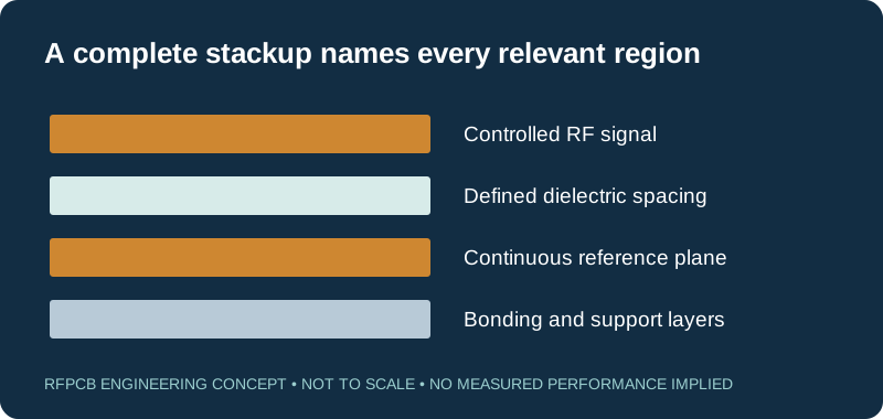
Inspect the RF return path and transitions
Follow the return path beneath and around the sensitive signal, not just the signal trace itself. Plane splits, voids, layer changes, connector launches and grounding around components can introduce discontinuities. Mark the regions that need electrical review rather than assuming a nominal impedance on a straight section covers them.
Include the enclosure, shield or carrier where it affects the circuit. For a dense design, review the interaction among signal vias, ground vias, antipads and nearby metal. DFM should identify fabrication constraints, while electromagnetic validation addresses the RF behavior of the resulting geometry.
Document holes, microvias and lamination sequence
A hole schedule should identify the start and end layers, nominal dimensions, plated or nonplated status and any fill or cap requirement. For HDI structures, include the build-up sequence and distinguish stacked from staggered microvias. A total board thickness cannot replace the dielectric depth used for microvia geometry review.
The HDI RF PCB page provides a geometry checker and a construction checklist. Its ratio result is not an automatic capability approval. Exact material, capture pad, taper, copper fill and reliability requirements remain part of the engineering assessment.
Call out RF-sensitive surface regions
Identify areas where solder mask is excluded, where a particular finish is needed and where dimensions are critical. Connector contacts, resonators, coupled lines and component grounds can need different consideration from general support circuitry. Include final copper assumptions when a model depends on them.
Review finish choices against electrical behavior, assembly and storage needs. A generic note such as “gold finish” may not identify the required finish stack. Use the RF finish guide to prepare specific questions and record the selected process in the fabrication drawing.
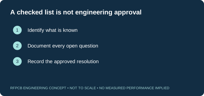
Separate fabrication DFM from assembly review
Bare-board manufacturability does not establish that components can be placed, soldered and inspected as intended. For assembly, provide the BOM, placement data, orientation marks, polarity, assembly drawings and any customer-supplied parts. Identify connectors, shields and mechanical hardware that affect access or test fixtures.
RF component reference layouts can contain electrically important details. Changes to grounding, matching or package surroundings should be reviewed by the circuit designer. Ask the assembly team to identify process concerns without silently changing sensitive geometry or substituting components that have not been approved.
Specify acceptance before requesting special tests
State what will be measured, on which article and against which limits. A bare-board electrical test checks different properties from an impedance coupon or an assembled RF sweep. Identify the fixture, calibration reference, frequency range and reporting requirements for any special measurement.
Use the quality and test page to organize the evidence request. For a filter, LNA or antenna, distinguish manufacturing evidence from complete circuit qualification. Agree who owns the RF validation work and include that scope in the quotation rather than assuming it is covered by a general test statement.
Close questions with a controlled engineering response
A useful DFM response states the issue, affected feature, proposed resolution and consequence for performance, cost or schedule. Group related questions so the designer can approve one consistent construction. Preserve the accepted answers alongside the final manufacturing files.
Use the interactive list below to prepare the first handoff. Downloaded notes remain your planning record and are not transmitted automatically. Once the package is complete, submit it through the quotation form and identify which questions still need a manufacturing proposal. Do not mark a design released while critical answers remain unresolved.
Prepare a reviewable engineering request
Check only the requirements you have actually documented. This list records readiness; it does not inspect your files or certify a design. Missing information is useful: identify it explicitly so the engineering review can resolve it before a production release.
These inputs are processed in your browser and are not submitted by this tool. The downloaded summary is a plain-text planning record. Use the secure quote form to send files; request an NDA first if your project requires one.
Manufacturing context
RFPCB and PCBSync share the manufacturing facility shown below. These process photographs illustrate the production environment; they are not evidence that a particular board, material grade or RF performance has been qualified. Request the documentation and inspection scope applicable to your project.



RF PCB DFM checklist FAQs
Does checking every item mean my PCB is manufacturable?
No. The checklist records whether you have prepared information. It does not inspect files, verify rules or approve a process. A manufacturer must review the actual construction and resolve the project-specific questions.
Is DFM the same as an RF design review?
They overlap but are different. DFM checks whether the proposed construction can be manufactured as specified. RF design validation addresses circuit behavior. A manufacturable line, via or filter can still fail its electrical target.
Can I upload confidential files into this checklist?
This tool does not accept or transmit files. Its notes and calculations stay in the browser until you copy or download them. Use the quote form for the intended submission and arrange an NDA first where required.
What is the best way to respond to supplier DFM questions?
Answer against one controlled revision, identify approved changes explicitly and update affected files. Preserve the final stackup and acceptance requirements with the response. Avoid conflicting approvals spread across several untracked messages.
Continue your engineering review
Send a package engineering can review
Download your preparation summary, attach the matching fabrication files and identify unresolved requirements. A clear package makes the manufacturing and quotation discussion more useful.
Sources and engineering scope
Manufacturer values apply to the identified grade, test method and construction. Engineering examples on this page are illustrative; they are not measured product results, inventory statements or certification claims. Rogers product names are trademarks of their owner. Keep the applicable datasheet revision with your approved manufacturing package.
Ready for a quotation?
Send your requirements for a material, stackup and manufacturing review. Price and schedule are confirmed for your project.