

RF performance · Loss budgeting and diagnosis
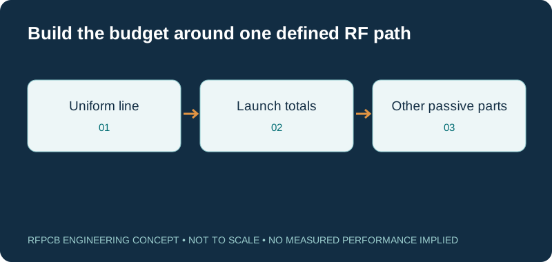
Reducing RF PCB loss starts by identifying where the signal power is lost or reflected. Define the operating band and measurement planes, then separate the uniform transmission line from connectors, transitions and other passive parts. Change the largest credible contribution first.
Shorten unnecessary RF routing, select an appropriate low-loss construction, review copper profile and line geometry, and improve discontinuities that cause reflection or radiation. Confirm the dominant mechanism before changing laminate. A lower Df alone does not guarantee lower connector-to-connector insertion loss, and arithmetic loss budgeting is only a planning approximation for matched or weakly reflecting paths.
Choose the intervention from the observed loss mechanism
| Observed concern | Candidate action | Evidence to obtain |
|---|---|---|
| Loss grows with route length | Review distributed attenuation and shorten routing | Representative line model or length comparison |
| Narrow line with large conductor contribution | Review geometry and foil profile together | Impedance-consistent construction comparison |
| Broad dielectric contribution | Compare exact low-loss material constructions | Applicable property data and routed-path result |
| Ripple or poor return loss | Inspect launches, vias and discontinuities | Full S-parameters and transition model |
| Difference between test setups | Review calibration and fixture treatment | Common reference planes and method |
| Loss changes with assembly state | Check connectors, shielding and geometry | Controlled assembled comparison |
RF route loss budget worksheet
Total = length × entered attenuation + total launch/transition allocation + other passive loss. Frequency labels the scenario; it does not synthesize an attenuation model. Use comparable data at that frequency and avoid counting the same feature twice. Adding scalar dB terms is a matched or weak-reflection planning approximation; use cascaded S-parameters for mismatched structures. Default values are illustrative.
Define insertion loss and the measurement boundary
Before comparing boards, draw the RF path and mark where the measurement starts and ends. State whether connectors, adapters, filters or test fixtures are included. Record the reference impedance and frequency range. A line-only prediction and a connectorized measurement can both be correct while answering different questions.
Under the usual matched-port convention, insertion loss is reported as a positive attenuation value derived from the magnitude of S21. It does not uniquely identify dielectric dissipation. Reflection, conductor loss and energy leaving the intended mode can reduce forward transmission too. Retain return-loss data and the full measurement context so diagnosis does not depend on a single attenuation number.
Use the loss-budget calculator without double counting
Enter distributed attenuation in dB/mm at the frequency being evaluated, then multiply it by route length. Add the combined launch loss and the total for other passive parts. The tool compares this arithmetic sum with your target and reports the remaining planning margin. Enter positive loss values and use consistent boundaries for every contribution.
For an illustrative case, 0.01 dB/mm over 50 mm contributes 0.50 dB. Adding 0.20 dB for all launches and 0.30 dB for other parts gives 1.00 dB. These are invented planning inputs, not material or factory results. If your line estimate already includes launches, do not enter those launches again.
Recognize when an arithmetic budget is insufficient
Adding loss magnitudes in decibels is useful for matched or weakly reflecting planning networks. It is not a complete cascade model for a path with substantial reflections. The relative phase of reflected waves can create frequency-dependent ripple and change the measured forward response. A scalar budget cannot reconstruct that interaction.
Use compatible complex S-parameters and appropriate network analysis when mismatch matters. Model transitions electromagnetically where their three-dimensional geometry is important. The calculator does not derive attenuation from Df, solve electromagnetic fields or estimate reflection from trace width. Treat an unexplained measurement discrepancy as a reason to examine the assumptions, not as justification for adjusting inputs until the sum matches.
Reduce unnecessary length before buying a new material
Trace the signal from its actual source to destination and identify detours introduced by placement, connector orientation or avoidable layer changes. Shortening a uniform lossy segment reduces its distributed contribution, provided the new route preserves the intended electrical structure. A compact layout that creates a poor launch or return-path interruption can lose that benefit.
Compare layout candidates using the same reference planes and assumptions. Preserve the component keepouts, assembly access and grounding needed by the product. For a receiver, the LNA PCB guide helps explain why the location of passive loss matters: an input-path improvement can have a different system consequence from the same change after substantial gain.
Balance dielectric, copper and impedance requirements
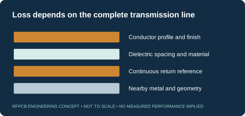
Rogers shows that conductor and dielectric contributions can have different importance as a controlled-impedance construction changes. Its circuit-loss discussion also demonstrates the influence of copper profile. Selecting a lower-Df material does not remove the need to evaluate the conductor system.
Compare complete candidate lines at the required impedance, including the resulting width and spacing. Keep copper identity and processing assumptions explicit. Use the RF material selection guide to structure the comparison. Avoid ranking unrelated datasheet values without checking their frequency, test method and construction, and request a representative result for the improvement you expect.
Choose line geometry with radiation and transitions in mind
Rogers’ millimeter-wave transmission-line guidance explains that microstrip radiation depends on substrate thickness and permittivity, and that transmission-line choices carry different tradeoffs. A thicker dielectric is therefore not an unconditional route to lower total loss, even when it allows a wider conductor at a given impedance.
Review connector pads, signal vias, return connections, plane openings and nearby enclosure features as part of the RF path. Specify the complete geometry before comparing simulations. The controlled-impedance page helps define straight-line targets; discontinuities and transitions still need their own electrical assessment.
Treat finish and assembly as controlled variables
Include the RF conductor finish and solder-mask arrangement in the baseline. When considering a finish change, discuss solderability, assembly sequence, storage and the electromagnetic model together. Do not assign a universal decibel penalty to a finish name without the construction and operating band that support it.
The RF surface-finish guide provides a framework for that decision. Inspect connector attachment and mechanical retention when comparing assembled boards, and keep the test connection repeatable. An apparent material improvement can be obscured by a changed connector interface, a different shield position or assembly variation that was never recorded in the comparison.
Measure a controlled experiment and verify the fixture
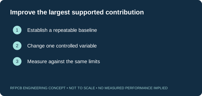
Keep a baseline and change one variable at a time. Agree the construction, sweep, calibration, connection method and limits. Use reference planes that match the requirement. Keysight explains that de-embedding removes characterized fixture effects using an appropriate model or measured data; it is not permission to subtract an arbitrary fixture loss.
Retain raw measurements as well as any processed result, with the fixture identity and method. Where coupons are used, document how they represent the product. Retain enough construction information to explain a repeatable difference.
Turn the improvement into a manufacturable specification
Rank candidate changes by expected electrical benefit, implementation effort and evidence needed. Request comparable quotations for the same acceptance scope, and use the RF PCB cost calculator to make commercial assumptions visible. Include another prototype or fixture when it is required to establish the benefit.
Submit the baseline stackup, proposed change, path drawing and measured concern through the engineering quote form. State whether the request concerns bare boards, a connectorized article or a populated assembly. Once a change is accepted, release the material, foil, geometry, finish and test requirements together so repeat orders preserve the construction that produced the approved result.
Prepare a reviewable engineering request
Check only the requirements you have actually documented. This list records readiness; it does not inspect your files or certify a design. Missing information is useful: identify it explicitly so the engineering review can resolve it before a production release.
These inputs are processed in your browser and are not submitted by this tool. The downloaded summary is a plain-text planning record. Use the secure quote form to send files; request an NDA first if your project requires one.
Manufacturing context
RFPCB and PCBSync share the manufacturing facility shown below. These process photographs illustrate the production environment; they are not evidence that a particular board, material grade or RF performance has been qualified. Request the documentation and inspection scope applicable to your project.


RF PCB loss reduction FAQs
Will a lower dissipation factor always reduce measured loss?
It may reduce the dielectric contribution for a comparable construction, but total forward loss also depends on copper, geometry, transitions, reflection and other components. Estimate the dominant terms before assuming the material change will meet the system target.
Can I add every component loss in dB?
Use that as a planning approximation for matched or weakly reflecting networks with consistent reference planes. Significant mismatch requires complex network analysis because reflected-wave phase and interactions are missing from a scalar sum.
Does the calculator predict loss from the laminate name?
No. You supply attenuation per millimeter and the other contributions. Obtain those inputs from suitable measurements, models or documented planning assumptions at the frequency of interest. The tool performs arithmetic and compares the result with your target.
What should I send for a loss-reduction review?
Send the stackup, material and foil details, RF path geometry, operating band, existing measurements and reference planes. Include connectors, finish, assembly state and the proposed acceptance limit so engineering can assess a concrete change.
Continue your engineering review
Request a review of your RF loss budget
Share the path, stackup, operating band and measurement boundaries. Identify the suspected contribution and the result needed so the proposed change can be evaluated against a clear baseline.
Sources and engineering scope
- Rogers: circuit materials and high-frequency PCB losses
- Rogers: transmission-line and material choices for millimeter waves
- Keysight: removing fixture effects from RF measurements
Manufacturer values apply to the identified grade, test method and construction. Engineering examples on this page are illustrative; they are not measured product results, inventory statements or certification claims. Manufacturer and product names belong to their respective owners. Keep the applicable datasheet revision with your approved manufacturing package.
Ready for a quotation?
Send your requirements for a material, stackup and manufacturing review. Price and schedule are confirmed for your project.