
Panasonic materials · Multilayer RF engineering
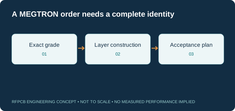
Panasonic MEGTRON PCB selection starts with the exact laminate and prepreg construction. A family name cannot define dielectric behavior, channel loss or manufacturing availability. Coordinate the material designation, copper and RF path before requesting a fabrication proposal.
Use MEGTRON as a candidate material family for a reviewed multilayer construction. Specify the series, grade suffix, core and prepreg details, glass style, resin content and foil. There is no single Dk for the entire family, and a high-speed material designation does not by itself qualify a particular RF circuit.
Turn a MEGTRON request into a defined construction
| Decision | Information to specify | Why it matters |
|---|---|---|
| Material identity | Series, laminate grade and suffix | Avoid an ambiguous family-level substitution |
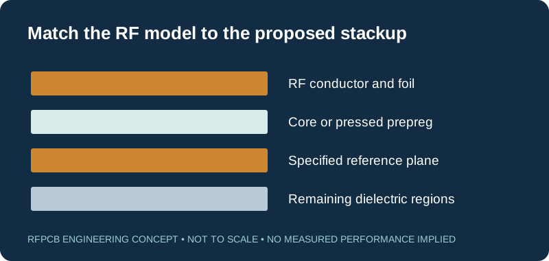
| Dielectric regions | Core and prepreg by layer pair | Connect the electrical model to the build |
| Glass and resin | Cloth style, ply count and resin content | Choose the applicable property reference |
| Copper system | Foil designation and finished thickness | Review conductor loss and geometry together |
| Electrical acceptance | Band, loss, impedance and phase limits | Define measurable project requirements |
| Commercial scope | Quantity, test article and allowed alternatives | Compare equivalent manufacturing proposals |
Route mismatch to phase and delay
Delay = length mismatch × √εeff / c; phase = 360 × frequency × delay. The effective permittivity belongs to the actual geometry, not a generic material family. This nondispersive estimate excludes bends, transitions and different route constructions.
MEGTRON6 suffixes describe meaningful differences
Panasonic identifies MEGTRON6 R-5775(N) with low-Dk glass and R-5775(K)/R-5775(G) with normal glass. Its product page gives typical 13 GHz reference Dk values of 3.34 and 3.62 respectively for the stated sample construction. Those are material references, not a universal impedance-model input. The manufacturer comparison also identifies the measurement conditions and warns that typical values are not guaranteed.
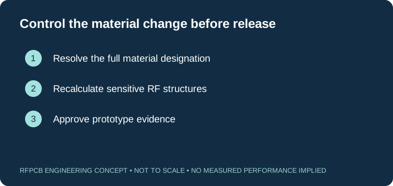
Preserve the suffix when copying a purchasing description into the stackup. Ask engineering to resolve a quotation that says only “MEGTRON6.” A missing identifier can hide an electrical change even when nominal dielectric thickness remains the same.
Read the construction table before selecting Dk
The R-5775(N) datasheet lists properties against glass style, ply count, resin content, thickness and frequency. Core and prepreg have separate construction tables. This is why a number copied from the top of a product page may not describe the dielectric region underneath your trace.
Create a stackup worksheet with one row for each electrically relevant region and a reference to the chosen datasheet row or supplier model. Record what remains provisional. When the proposed pressed construction changes, update the model and review its effect before approving the revised drawing. The material selection guide helps organize these comparisons.
Assess RF and digital paths using their own requirements
A mixed-signal board can contain a long digital channel, a short microwave feed and a sensitive clock distribution network. They do not necessarily rank material changes in the same order. Give each path a requirement that can be checked: channel attenuation, phase balance, impedance, isolation or a defined combination.
Use the multilayer RF PCB guide to describe the layer arrangement and reference planes. Mark where an RF route changes layers or crosses between construction regions. Reviewing the sensitive paths first makes it easier to judge whether a proposed stackup change solves the actual design problem and whether another path needs revalidation.
Use the delay tool to explore length mismatch
The tool estimates the delay difference produced by a physical length mismatch using an assumed effective permittivity. For mismatch ΔL, delay is ΔL × √εeff / c; phase difference at a selected frequency follows from that delay. Enter effective permittivity for the guided structure, with consistent units, rather than treating a published bulk Dk as an automatic substitute.
This is an ideal sensitivity calculation. It excludes dispersive behavior, different propagation environments, via delays and connector asymmetry. Equal physical lengths can still have unequal electrical delays. For a phase-sensitive array or coherent receiver, retain the complete path model and check the assembled response over the required band.
Choose foil and geometry alongside the dielectric
A material review should contain enough information to reconstruct the transmission line. Request the foil designation, finished conductor thickness, dielectric spacing, trace dimensions and surface treatment. Keep the intended impedance and reference plane beside those values so the reviewer can identify coupled changes.
If lower attenuation motivates the choice, compare representative paths on the proposed builds instead of ordering from a Df ranking. A narrow route, a long route and a connector transition pose different questions. Use the RF PCB loss guide to divide the budget into line, launch and component contributions, then obtain the models or measurements needed for the dominant items.
Review the complete bonding and multilayer proposal
A multilayer drawing needs more than the selected core grade. Include the bonding materials, intended pressed separations, copper distribution and any sequential processing requirements. Ask the fabricator to identify the proposed construction explicitly, including details that remain subject to material sourcing or engineering review.
Where RF and support layers have different needs, evaluate a hybrid stackup as a separate candidate. Its cost and electrical behavior depend on the full build. Keep the approved RF reference region visible in every alternative and avoid authorizing a material substitution through a vague note such as “equivalent low-loss laminate acceptable.”
Separate material cost from finished-board economics
Request comparable prices for the same revision, quantities, copper, finish, inspection and delivery scope. A quotation should identify its material assumption and explain whether engineering changes are included. Do not infer stock, minimum order or lead time from a manufacturer datasheet or from the existence of a material guide.
The RF PCB cost calculator can compare confirmed commercial inputs and explicit planning assumptions. Include qualification effort when considering a new grade for an established product. A modest unit-price difference may have little value if another prototype, fixture or approval cycle is needed before production can use the alternative.
Specify evidence that answers the project question
Choose a test article that represents the concern. A controlled-impedance coupon addresses a different question from a routed insertion-loss coupon, a phase-matched network or a populated RF assembly. Define which layers, transitions and surface treatments must be represented and which items are excluded.
Agree the frequency range, measurement boundaries, sample quantity and report content before ordering. If a supplier proposes a standard coupon, compare its construction with the actual sensitive route. Keep measured data with the board revision and stackup so later reviewers can distinguish material identity checks, geometric inspection and RF performance evidence without reconstructing the project from scattered messages.
Prepare a MEGTRON manufacturing request
Submit the fabrication files, stackup, quantities and exact material designation through the project quote form. Identify whether the request is for feasibility, prototype fabrication or repeat production. List approved alternatives separately from grades that still need investigation, and attach the acceptance plan when RF measurements are part of the deliverable.
For a repeat order, reference the accepted construction and report any changes in layout, finish or assembly. Retain the approved material row and supplier response with the released drawing. That record gives purchasing a practical basis for reviewing later availability-driven proposals while preserving the electrical assumptions that supported the original approval.
Prepare a reviewable engineering request
Check only the requirements you have actually documented. This list records readiness; it does not inspect your files or certify a design. Missing information is useful: identify it explicitly so the engineering review can resolve it before a production release.
These inputs are processed in your browser and are not submitted by this tool. The downloaded summary is a plain-text planning record. Use the secure quote form to send files; request an NDA first if your project requires one.
Manufacturing context
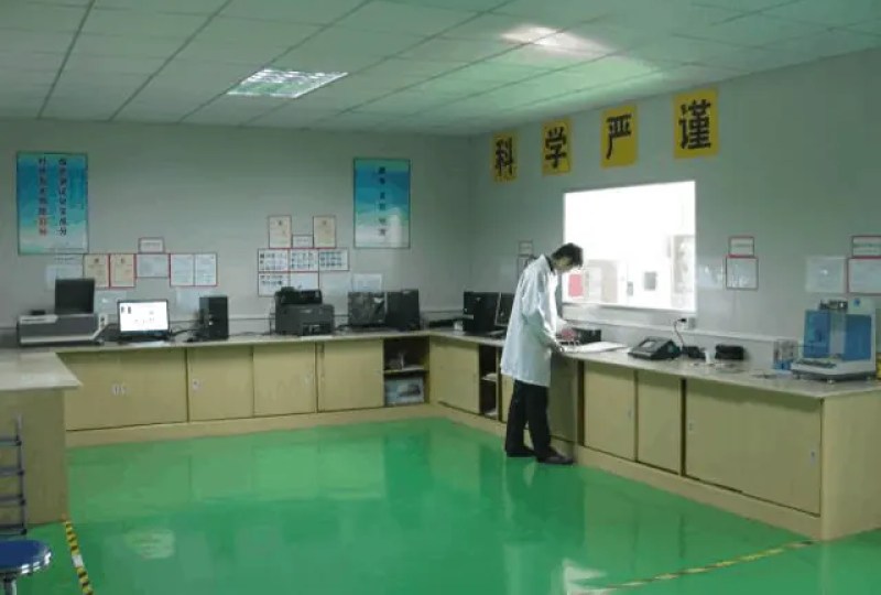
RFPCB and PCBSync share the manufacturing facility shown below. These process photographs illustrate the production environment; they are not evidence that a particular board, material grade or RF performance has been qualified. Request the documentation and inspection scope applicable to your project.


Panasonic MEGTRON PCB FAQs
What is the dielectric constant of MEGTRON PCB material?
There is no single value for the family. Select the exact series, suffix and construction, then keep the test method and frequency with the property. The effective permittivity of a transmission structure also depends on its geometry.
Can MEGTRON replace Rogers without changing the layout?
A substitution requires a construction-specific electrical and fabrication review. Compare the relevant paths, geometry, loss, phase and acceptance results. Identical artwork or similar nominal Dk does not establish equivalence.
Does this page confirm that every MEGTRON grade is available?
No. Grade, thickness, foil, quantity and sourcing must be confirmed in the project proposal. Manufacturer product literature and an engineering guide do not establish current factory inventory or an approved process for every construction.
Does the delay calculator predict channel skew?
It predicts the ideal contribution from a specified length mismatch in one assumed propagation environment. Different layer environments, dispersion, vias, launches and coupling require additional modeling and appropriate verification.
Continue your engineering review
Request a construction-specific MEGTRON review
Send the complete material designation, proposed stackup and sensitive-path requirements. Request a documented manufacturing proposal with sourcing assumptions and acceptance scope.
Sources and engineering scope
- Panasonic circuit-board-material technical support and datasheets
- Panasonic MEGTRON6 grade and glass-system comparison
- Panasonic R-5775(N) construction-specific laminate and prepreg data
Manufacturer values apply to the identified grade, test method and construction. Engineering examples on this page are illustrative; they are not measured product results, inventory statements or certification claims. Manufacturer and product names belong to their respective owners. Keep the applicable datasheet revision with your approved manufacturing package.
Ready for a quotation?
Send your requirements for a material, stackup and manufacturing review. Price and schedule are confirmed for your project.