

What Is an RF PCB Prototype and Why Does Quantity Matter?
An RF PCB prototype is a small-quantity board run—typically 5 to 25 pieces—built on controlled-impedance high-frequency laminates so you can validate transmission-line performance, antenna patterns, and filter responses before committing to volume. Because RF laminates like Rogers RO4350B (Dk 3.48 ± 0.05) or Rogers RO3003G2 (Dk 3.00) cost 8–40× more per panel than standard FR-4, the economics of prototyping are fundamentally different from digital boards. Every extra panel matters, and getting the design right the first time saves weeks and thousands of dollars.
This guide walks through the decisions that separate a successful RF PCB prototype from an expensive paperweight: material selection, stackup planning, minimum-order economics, DFM review, post-assembly cleaning, and the handoff to production.
Material Selection for RF Prototypes

Matching Laminate to Frequency Band
The laminate you choose sets the ceiling on every electrical parameter. A general rule: the higher the operating frequency, the lower the dissipation factor (Df) you need, and the tighter the Dk tolerance must be to hold impedance across a production panel.
| Frequency Band | Typical Laminate | Dk / Df (10 GHz) | Common Application |
|---|---|---|---|
| Sub-6 GHz | Rogers RO4350B | 3.48 / 0.0037 | 5G sub-6 filters, Wi-Fi 6E front-ends |
| 6–30 GHz | Rogers RO3003G2 | 3.00 / 0.0010 | Ku-band satcom, radar IF boards |
| 30–77 GHz | Rogers RO3003 | 3.00 / 0.0013 | 77 GHz automotive radar, 5G mmWave |
| 77 GHz+ | Isola Astra MT77 | 3.00 / 0.0017 | Imaging radar, E-band backhaul |
For prototypes below 6 GHz, RO4350B is often the best trade-off: it processes on standard FR-4 equipment (no special PTFE drill bits or plasma desmear), ships in standard panel sizes, and is widely stocked. Above 10 GHz, pure PTFE or ceramic-filled PTFE laminates become necessary, but they require shops experienced with soft-substrate handling—mishandling causes resin smear in vias and delamination at reflow.
Hybrid Stackups: Cost Control Without Compromise
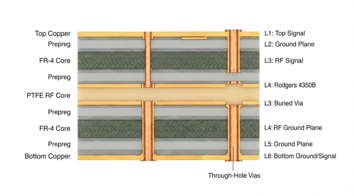
A common prototype strategy is a hybrid stackup: RF-critical signal layers on a high-frequency core, with FR-4 or low-cost prepreg for power and digital layers. This can cut raw material cost by 30–50 % compared to an all-PTFE build while keeping transmission-line loss within budget. The catch is that the bond between dissimilar materials must be validated—CTE mismatch (FR-4 z-axis CTE ~60 ppm/°C vs. PTFE ~25 ppm/°C) can crack via barrels during thermal cycling. Ask your fabricator for a stackup design review before locking the layer assignment.
Minimum Order Quantity and Panel Economics
Why “No MOQ” Still Has a Minimum Cost
Most RF-capable fabricators will quote as few as 5 pieces, but the real economic unit is the panel, not the board. A standard fabrication panel is 18 × 24 in (457 × 610 mm). If your prototype is 2 × 3 in (50 × 75 mm), roughly 24 pieces fit on one panel after routing margins. Ordering 5 pieces means the other 19 array positions are either wasted or filled with other customers’ boards in a shared-panel run.
Understanding this panel math lets you negotiate smarter. Ordering 10 instead of 5 may cost only 10–15 % more because the panel is already being processed. Conversely, ordering 25 of a large board may push you onto a second panel and nearly double the price. Use the optimizer below to explore how quantity interacts with unit cost for your board dimensions.
If the tool shows that 10 pieces costs only marginally more than 5, order the extras—you will want spare boards for destructive cross-sectioning, coupon testing, or a second assembly iteration without re-ordering bare boards. For deeper context on how panel utilization drives RF board pricing, see the minimum order guide for RF PCB prototypes.
DFM Review: The Step That Prevents Respins
An RF prototype that fails because of a manufacturing error—not a design error—is the most expensive kind of failure, because you learn nothing from it. A thorough DFM review for RF PCBs catches issues that generic design-rule checks miss.
Critical RF DFM Checks
- Trace-width tolerance vs. impedance sensitivity. A 50 Ω microstrip on RO4350B (18 mil / 0.46 mm wide on 10 mil / 0.254 mm dielectric) shifts about 2 Ω per mil of width variation. If the fab’s etch tolerance is ± 1 mil, your worst-case impedance is 48–52 Ω—acceptable for most systems. On thinner dielectrics or at higher Dk, the sensitivity is steeper, so tighter etch classes or impedance modeling verification may be needed.
- Via-to-trace clearance on ground planes. Anti-pads that are too large create impedance discontinuities in the reference plane. Keep anti-pad diameter ≤ 1.5× the drill diameter for signal vias, and use via fences with pitch ≤ λ/10 around microstrip-to-stripline transitions.
- Copper-to-edge clearance for PTFE routing. Soft PTFE substrates require controlled-depth routing or laser depaneling to avoid burring. Copper features closer than 15 mil (0.38 mm) to the board edge risk smearing during routing. For more on this, see the RF PCB depaneling guide.
- Soldermask over RF traces. Soldermask has a Dk of roughly 3.5–4.2 and adds a dielectric loading effect that shifts impedance by 2–5 Ω depending on thickness. Either mask-relieve all RF traces or model the mask in your impedance simulation.
- Drill aspect ratio. IPC-6012 Class 2 allows a maximum drill aspect ratio of 10:1. A 6-mil (0.15 mm) laser-drilled microvia in a 10-mil core is fine, but a mechanically drilled 8-mil via through a 100-mil board (12.5:1) will be rejected or require sequential lamination.
What a Good DFM Report Delivers
Expect the report within 12–24 hours of submitting Gerbers. It should flag each issue with a screenshot, the affected layer, the violated rule, and a recommended fix. Critically, it should also confirm controlled-impedance structures and their modeled values against your target, referencing IPC-6012 class requirements where applicable.
Assembly Cleaning: No-Clean vs. Aqueous Wash
Why This Decision Matters More for RF
Flux residue is a dielectric. On a digital board, a thin no-clean residue film is electrically invisible. On an RF board operating above a few GHz, that same residue sitting on a coupled-line filter or between the pads of a 0201 matching network can shift resonant frequency by tens of MHz and increase insertion loss by 0.1–0.3 dB. The higher the frequency, the worse the effect—at 77 GHz, even fingerprint oils are measurable.
The trade-off is that aqueous washing introduces its own risks: water ingress under shielding cans, ionic contamination if rinse quality is poor, and potential damage to exposed wire-bond pads. Use the tool below to weigh the factors for your specific prototype.
If the tool recommends aqueous wash—common for prototypes above 10 GHz or with tight filter specifications—make sure the assembly house uses DI water with resistivity above 10 MΩ·cm and confirms drying with ionic contamination testing per IPC J-STD-001 limits (≤ 1.56 µg NaCl/cm² equivalence for Class 3). For prototypes heading to an RF PCB assembly service, specify the cleaning requirement on the purchase order—don’t assume it’s included.
Prototype Build Options and Lead Times
Quick-Turn vs. Standard Cycle
| Service Tier | Typical Lead Time (Bare Board) | Best For | Cost Premium |
|---|---|---|---|
| Quick-turn | 5–7 working days | First-spin validation, trade-show demos | 30–60 % over standard |
| Standard | 10–15 working days | Second-spin refinement, cost-sensitive R&D | Baseline |
| Expedite | 3–4 working days | Emergency respins, program-critical deadlines | 80–150 % over standard |
Lead times assume the laminate is in stock. RO4350B in 10 and 20 mil thicknesses is almost always available. Specialty laminates like RO3006 or Taconic TLY-5 may add 2–4 weeks of material lead time on top of fabrication. Confirm stock before placing the order.
Surface Finish for RF
ENIG (electroless nickel / immersion gold) is the default for RF prototypes: it provides a flat, solderable surface with good shelf life. However, the nickel underlayer (typically 3–6 µm) is ferromagnetic and increases skin-effect loss above ~10 GHz. For millimeter-wave work, consider immersion silver or OSP with immediate assembly. Hard gold plating (30–50 µin / 0.76–1.27 µm) is preferred for edge-launch connector pads and test-probe contact areas.
From Prototype to Production: Planning the Transition
A prototype proves the design works. Transferring it to volume production proves the process works—repeatably. The most common mistakes in the prototype-to-production handoff are:
- Changing fabricators without re-qualifying impedance. Different shops use different etch chemistries and stackup presses. A 50 Ω line validated at one shop may measure 47 Ω at another. Always request impedance coupons on the first production panel.
- Tightening tolerances without cost impact analysis. Moving from IPC Class 2 to Class 3 adds 15–30 % to bare-board cost and may require additional testing (microsection, solderability, thermal stress). Make sure the application genuinely needs it.
- Ignoring panel utilization. A prototype board outline optimized for bench testing (irregular shape, large keep-outs) may waste half the panel at volume. Redesigning the outline or adding breakaway tabs early saves significant cost at 500+ pieces.
If the end application is defense or aerospace, ensure the prototype build already follows ITAR-compliant data handling and the appropriate Rogers material specification so qualification data carries forward.
Checklist: Ordering Your RF PCB Prototype
- Lock the stackup. Confirm laminate, prepreg, copper weight, and dielectric thickness with the fabricator’s stackup tool before generating Gerbers.
- Run a full DFM review. Submit Gerbers, drill files, impedance table, and the fabrication drawing. Expect feedback within 12–24 hours.
- Specify impedance targets on the fab drawing. Include target impedance, tolerance (typically ± 10 % for prototype, ± 5 % for production), and reference to the coupon test method (IPC-TM-650, method 2.5.5.7).
- Choose quantity based on panel economics. Use the MOQ optimizer above to find the sweet spot.
- Confirm laminate stock. A 2-week material delay defeats the purpose of a quick-turn prototype.
- Decide cleaning method before assembly. Use the no-clean vs. wash tool to match the method to your frequency and reliability requirements.
- Request impedance test coupons and a microsection report. Even on a 5-piece prototype, one coupon per impedance class is standard practice.
- Archive the complete build package. Gerbers, drill files, stackup, impedance report, and any DFM waivers—this package is your baseline for the production transfer.
FAQ
Can I prototype an RF board on FR-4?
Below about 1 GHz, standard FR-4 (Dk ~4.3, Df ~0.020 at 1 GHz) can work for non-critical RF paths like GPS L1 patches or sub-GHz ISM antennas. Above 2 GHz, the Dk variation across a panel (± 10 % is common) and high loss make FR-4 unsuitable for anything requiring repeatable impedance or low insertion loss.
What is the smallest practical RF PCB prototype order?
Five pieces is a common minimum. Some fabricators accept as few as one, but the per-unit cost is extreme because you still pay for a full panel setup. Ordering 5–10 pieces gives you enough boards for assembly, testing, cross-section verification, and spares.
How tight can impedance tolerance be on a prototype run?
± 10 % is standard for prototype quantities. Achieving ± 5 % is possible but requires tighter etch control, coupon-verified dielectric thickness, and sometimes a test-and-sort step that adds cost and time. Reserve ± 5 % for production runs where statistical process control is in place.
Should I add a conformal coating at the prototype stage?
Generally, no—conformal coating adds a dielectric layer over traces that shifts impedance and must be characterized. Test the bare board first to isolate electrical performance from coating effects. If the end product requires coating for environmental protection, add it in a second prototype spin after the RF design is validated.
How do I transition from 5-piece prototype to 500-piece production?
Start by locking the qualified stackup and impedance coupon data from the prototype run. Re-panelize for volume efficiency, confirm the production fabricator can hold the same etch and registration tolerances, and run a first-article inspection (FAI) on the initial production panel. This handoff is where most schedule and yield surprises happen—plan two weeks for it.
Ready for a quotation?
Send your requirements for a material, stackup and manufacturing review. Price and schedule are confirmed for your project.