Introduction to PCB stencils
A PCB (Printed Circuit Board) stencil is a thin sheet of metal, usually stainless steel or nickel, with precise laser-cut openings that correspond to the pads on a PCB. The purpose of a PCB stencil is to accurately apply solder paste to the pads of a PCB before components are placed and the board is reflowed in an oven. This process is known as Solder paste printing or stencil printing.
PCB stencils are an essential tool in the surface mount technology (SMT) assembly process, ensuring consistent and precise application of solder paste. This leads to higher quality solder joints, fewer defects, and improved reliability of the assembled PCB.
Key features of PCB stencils:
- Material: Stainless steel or nickel
- Thickness: Typically 0.1 mm to 0.2 mm (100 to 200 microns)
- Aperture design: Laser-cut openings matching PCB pad layout
- Mounting: Frameless or framed for compatibility with printing equipment
Importance of PCB Stencils in Electronics Manufacturing
PCB stencils play a crucial role in the electronics manufacturing process, particularly in surface mount assembly. Some key reasons why PCB stencils are important include:
-
Consistency: Stencils ensure a consistent amount of solder paste is applied to each pad on the PCB, reducing the risk of defects caused by insufficient or excessive solder.
-
Precision: Laser-cut stencils provide high precision in applying solder paste, ensuring the paste is deposited accurately on the pads, even for fine-pitch components.
-
Efficiency: Stencil printing is a fast and efficient method for applying solder paste to a large number of PCBs, making it suitable for high-volume production.
-
Cost-effectiveness: Using PCB stencils reduces the amount of solder paste waste and minimizes the need for rework, leading to cost savings in the manufacturing process.
-
Improved reliability: Consistent and precise solder paste application leads to higher quality solder joints, improving the overall reliability of the assembled PCB.

PCB Stencil Design Considerations
Designing a PCB stencil involves several key considerations to ensure optimal performance and compatibility with the PCB and assembly process. These include:
Stencil thickness
The thickness of the stencil determines the amount of solder paste deposited on the pads. Thicker stencils deposit more paste, which is suitable for larger components or pads. Thinner stencils are used for smaller components or fine-pitch applications. Common stencil thicknesses range from 0.1 mm to 0.2 mm (100 to 200 microns).
Aperture design
Apertures are the openings in the stencil that allow solder paste to be deposited on the PCB pads. The size and shape of the apertures should be designed to match the size and shape of the corresponding pads on the PCB. Aperture design factors include:
- Size: Aperture size is typically 1:1 with the pad size but can be adjusted based on the solder paste and printing process requirements.
- Shape: Apertures can be round, square, rectangular, or custom-shaped to match the pad design.
- Pitch: The distance between apertures should match the pitch of the components and pads on the PCB.
Stencil material
PCB stencils are most commonly made from stainless steel or nickel. Stainless steel is the most widely used material due to its durability, stability, and cost-effectiveness. Nickel stencils are used in applications that require finer apertures or improved wear resistance.
Mounting options
PCB stencils can be frameless or framed, depending on the requirements of the printing equipment and process.
- Frameless stencils: These stencils are used with dedicated stencil printing machines that have a built-in tensioning system.
- Framed stencils: These stencils are mounted in a frame, which provides stability and allows for easy handling and storage. Framed stencils are compatible with a wider range of printing equipment.

PCB Stencil Manufacturing Process
The manufacturing process for PCB stencils involves several key steps to ensure the stencils meet the required specifications and quality standards. These steps include:
-
Design and data preparation: The PCB stencil design is created based on the PCB layout and component requirements. The design data is then prepared for the manufacturing process, which involves converting the data into a format compatible with the laser cutting machine.
-
Material selection: The appropriate stencil material (stainless steel or nickel) is selected based on the application requirements and desired stencil thickness.
-
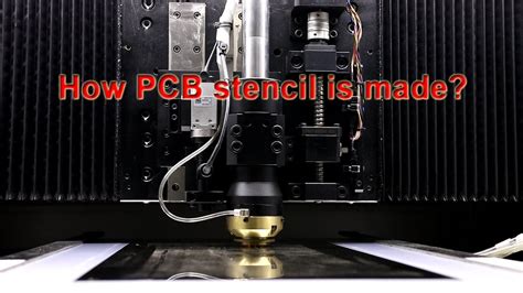
Laser cutting: A high-precision laser cuts the stencil according to the prepared design data. The laser vaporizes the material, creating the apertures and cutting the stencil to the required size and shape.
-
Cleaning: After laser cutting, the stencil is cleaned to remove any debris or contamination from the manufacturing process. This ensures the stencil is ready for use in the printing process.
-
Inspection: The stencil is inspected to ensure it meets the required specifications, including aperture size, shape, and position. Optical inspection systems are commonly used to verify the accuracy of the stencil.
-
Packaging: The finished stencil is packaged for protection during storage and transportation. Frameless stencils are typically packaged in protective sleeves, while framed stencils are packaged in boxes or crates.
Laser cutting technology
Laser cutting is the most common method for manufacturing PCB stencils. Laser cutting offers several advantages over other methods, such as chemical etching or electroforming:
- Precision: Laser cutting provides high precision, with the ability to create apertures as small as 0.1 mm (100 microns) with tight tolerances.
- Speed: Laser cutting is a fast process, allowing for quick turnaround times and high-volume production.
- Flexibility: Laser cutting can accommodate a wide range of stencil designs, including custom aperture shapes and sizes.
- Consistency: Laser cutting ensures consistent results across multiple stencils, as the process is highly repeatable.

Solder Paste Printing Process
The solder paste printing process is a critical step in surface mount assembly, where the PCB stencil is used to apply solder paste to the pads on the PCB. The process involves several key steps:
-
Stencil alignment: The PCB stencil is aligned with the PCB using fiducial marks or alignment pins to ensure precise registration between the stencil apertures and the PCB pads.
-
Solder paste application: Solder paste is applied to the top surface of the stencil, typically using an automated dispensing system or a manual squeegee.
-
Printing: The solder paste is forced through the stencil apertures onto the PCB pads using a squeegee. The squeegee is moved across the stencil at a controlled speed and pressure to ensure consistent paste deposition.
-
Stencil removal: After printing, the stencil is carefully removed from the PCB, leaving the solder paste deposits on the pads.
-
Inspection: The PCB is inspected after solder paste printing to ensure the paste deposits are consistent, properly aligned, and free from defects such as bridging or insufficient paste.
Factors affecting solder paste printing quality
Several factors can impact the quality of the solder paste printing process, including:
-
Stencil design: The stencil design, including aperture size, shape, and pitch, must be optimized for the specific PCB layout and components to ensure consistent paste deposition.
-
Solder paste properties: The solder paste must have the appropriate viscosity, particle size, and flux chemistry for the specific application and printing process.
-
Printing parameters: The printing speed, pressure, and separation speed must be optimized to ensure consistent paste deposition and minimize defects.
-
Environmental conditions: Temperature and humidity can affect the solder paste’s rheology and printing performance, so these conditions must be controlled during the printing process.
PCB Stencil Maintenance and Cleaning
Proper maintenance and cleaning of PCB stencils are essential for ensuring consistent solder paste printing quality and extending the stencil’s life. Key aspects of stencil maintenance and cleaning include:
Cleaning frequency
PCB stencils should be cleaned regularly to remove solder paste residue and prevent the buildup of contamination. The cleaning frequency depends on several factors, including:
- Solder paste type: Some solder pastes are more prone to drying or leaving residue on the stencil, requiring more frequent cleaning.
- Production volume: Higher production volumes will necessitate more frequent stencil cleaning.
- Environmental conditions: Higher temperatures and humidity can accelerate solder paste drying and residue buildup.
Cleaning methods
There are several methods for cleaning PCB stencils, including:
- Manual cleaning: This involves using solvents and wiping materials to manually clean the stencil. This method is suitable for low-volume production or quick cleaning between prints.
- Ultrasonic cleaning: Ultrasonic Cleaners use high-frequency sound waves to agitate a cleaning solution, effectively removing solder paste residue from the stencil. This method is more thorough and efficient than manual cleaning.
- Automated cleaning: Automated stencil cleaning systems use a combination of solvents, brushes, and air knives to clean the stencil. These systems are suitable for high-volume production and provide consistent cleaning results.
Stencil storage
When not in use, PCB stencils should be stored properly to prevent damage and contamination. Frameless stencils should be stored in protective sleeves, while framed stencils should be stored in a dry, dust-free environment. Proper storage helps extend the stencil’s life and ensures it is ready for use when needed.
Troubleshooting Common PCB Stencil Issues
Despite best practices in design, manufacturing, and maintenance, issues can still arise with PCB stencils. Some common issues and their potential solutions include:
Solder paste bridging
Solder paste bridging occurs when the paste deposits on adjacent pads are connected, causing a short circuit. Causes and solutions include:
- Stencil aperture size: If the apertures are too large, reduce the size to minimize paste spreading.
- Solder paste viscosity: If the paste is too thin, switch to a higher viscosity paste to reduce spreading.
- Printing parameters: Adjust the printing speed, pressure, and separation speed to optimize paste deposition.
Insufficient solder paste deposition
Insufficient solder paste deposition can lead to weak solder joints or open circuits. Causes and solutions include:
- Stencil aperture size: If the apertures are too small, increase the size to allow more paste to be deposited.
- Stencil thickness: If the stencil is too thin, consider using a thicker stencil to increase paste volume.
- Solder paste viscosity: If the paste is too thick, switch to a lower viscosity paste to improve flow through the apertures.
Stencil damage
Stencil damage, such as bent or torn apertures, can cause inconsistent paste deposition and defects. Causes and solutions include:
- Handling: Ensure proper handling techniques are used to prevent damage during stencil installation and removal.
- Cleaning: Use appropriate cleaning methods and solvents to avoid damaging the stencil.
- Storage: Store stencils properly to prevent damage during storage and transportation.
Frequently Asked Questions (FAQ)
-
What is the difference between a PCB stencil and a solder paste mask?
A PCB stencil is a separate, laser-cut sheet of metal used to apply solder paste to the pads on a PCB. A solder paste mask, also known as a solder resist or solder mask, is a layer applied directly to the PCB that covers the non-pad areas to prevent solder from adhering to those areas during the reflow process. -
How often should I clean my PCB stencil?
The cleaning frequency for PCB stencils depends on factors such as the solder paste type, production volume, and environmental conditions. As a general guideline, stencils should be cleaned every 4-8 hours of continuous use or between shifts. However, more frequent cleaning may be necessary for high-volume production or when using solder pastes prone to drying or leaving residue. -
Can I reuse a PCB stencil for different PCB designs?
No, each PCB stencil is designed specifically for a particular PCB layout and component set. The stencil apertures are precisely aligned with the pads on the PCB, so using a stencil designed for a different PCB will result in misaligned solder paste deposits and defects. -
What is the typical lifespan of a PCB stencil?
The lifespan of a PCB stencil depends on factors such as the stencil material, production volume, and maintenance practices. On average, a well-maintained stainless steel stencil can last for 50,000 to 100,000 prints, while a nickel stencil can last up to 250,000 prints. However, the actual lifespan may vary based on the specific application and usage conditions. -
Can I use a damaged or worn PCB stencil?
No, using a damaged or worn PCB stencil can lead to inconsistent solder paste deposition, defects, and reduced PCB quality. If a stencil is damaged or shows signs of wear, such as enlarged or deformed apertures, it should be replaced to ensure optimal printing results.
In conclusion, PCB stencils are an essential tool in the surface mount assembly process, ensuring consistent and precise solder paste deposition for high-quality PCB manufacturing. By understanding the design, manufacturing, and maintenance aspects of PCB stencils, engineers and manufacturers can optimize their PCB Assembly processes, reduce defects, and improve overall product reliability.
Leave a Reply