Introduction to Solder Paste Printing in SMT Assembly
Solder paste printing is a critical step in surface mount technology (SMT) assembly, where solder paste is precisely deposited onto the printed circuit board (PCB) pads before placing the electronic components. The accuracy and consistency of solder paste printing significantly impact the quality and reliability of the final assembled PCB. In this comprehensive article, we will explore what solder paste is, its composition, and the various aspects of the solder paste printing process in SMT assembly.
What is Solder Paste?
Solder paste is a grey, paste-like material consisting of tiny solder particles suspended in a flux medium. It is used to establish electrical and mechanical connections between electronic components and the PCB. The solder particles in the paste are typically made of a tin-lead (SnPb) alloy or lead-free alloys like tin-silver-copper (SAC).
Composition of Solder Paste
Solder paste consists of two main components:
-
Solder alloy particles: These particles make up 85-90% of the solder paste by weight. The size of the particles ranges from 25-45 microns, depending on the application and the desired printing resolution.
-
Flux medium: The flux medium is a complex mixture of ingredients, including rosins, activators, solvents, and other additives. It serves multiple purposes, such as removing oxides from the metal surfaces, preventing reoxidation, and promoting the flow and wetting of the molten solder during the reflow process.
Solder Paste Properties
The performance of solder paste depends on several key properties:
-
Viscosity: Viscosity is a measure of the solder paste’s resistance to flow. It determines the ease of printing and the ability to maintain the desired shape after printing. The viscosity of solder paste is affected by factors such as temperature, shear rate, and particle size distribution.
-
Tackiness: Tackiness refers to the ability of the solder paste to hold components in place after placement and before reflow. It prevents component movement during handling and transportation.
-
Slump resistance: Slump resistance is the ability of the printed solder paste to maintain its shape and dimensions without spreading or collapsing. It is essential for achieving accurate and consistent solder joints.
-
Shelf life: Shelf life is the length of time that solder paste can be stored without deteriorating in quality. It is affected by factors such as storage temperature, humidity, and packaging.

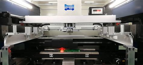
Solder Paste Printing Process
The solder paste printing process involves several steps and considerations to ensure optimal results.
Stencil Design
A stencil is a thin metal sheet with apertures that correspond to the PCB pads where solder paste needs to be deposited. The stencil design is crucial for achieving the desired solder paste volume and shape.
Factors to consider in stencil design include:
-
Aperture size and shape: The aperture size and shape should match the PCB pad size and shape, taking into account the desired solder paste volume and the component type.
-
Stencil thickness: The stencil thickness determines the height of the printed solder paste. Typical stencil thicknesses range from 100-150 microns, depending on the component package and the required solder joint height.
-
Aperture wall tapering: Tapering the aperture walls can facilitate the release of the solder paste during printing and improve the print quality.
Printer Setup and Calibration
Before printing, the solder paste printer needs to be properly set up and calibrated to ensure accurate and consistent results.
Key aspects of printer setup and calibration include:
-
Alignment: The stencil and PCB should be accurately aligned to ensure that the solder paste is deposited on the correct pads.
-
Squeegee pressure and speed: The pressure and speed of the squeegee affect the solder paste deposition and the print quality. Optimal settings depend on factors such as the solder paste type, stencil design, and PCB surface finish.
-
Printer parameters: Other printer parameters, such as snap-off distance, print gap, and separation speed, should be optimized for the specific application and solder paste type.
Printing Process
The actual printing process involves the following steps:
-
Solder paste dispensing: Solder paste is placed on the stencil surface, typically using an automated dispenser.
-
Squeegee motion: The squeegee blade moves across the stencil, forcing the solder paste through the apertures and onto the PCB pads.
-
Stencil separation: After printing, the stencil is separated from the PCB, leaving the solder paste deposits on the pads.
-
Inspection: The printed PCB is inspected, either manually or using automated optical inspection (AOI) systems, to verify the solder paste deposit quality and identify any defects.
Printing Defects and Troubleshooting
Several types of defects can occur during solder paste printing, affecting the quality and reliability of the solder joints. Common printing defects include:
-
Insufficient or excessive solder paste: This can lead to open circuits, shorts, or poor joint strength.
-
Bridging: Solder paste bridging between adjacent pads can cause short circuits.
-
Scooping: Scooping occurs when the solder paste is pulled out of the aperture during stencil separation, resulting in incomplete or inconsistent deposits.
-
Slumping: Slumping refers to the spreading or collapse of the printed solder paste, which can cause bridging or insufficient solder joint volume.
Troubleshooting printing defects involves identifying the root cause and implementing appropriate corrective actions, such as adjusting printer parameters, modifying stencil design, or optimizing solder paste properties.

Best Practices for Solder Paste Printing
To achieve optimal solder paste printing results, consider the following best practices:
-
Solder paste storage and handling: Store solder paste in a controlled environment, following the manufacturer’s recommendations for temperature and humidity. Ensure proper handling to prevent contamination and maintain consistent properties.
-
Stencil maintenance: Regularly clean and inspect the stencil to prevent clogging and maintain print quality. Use appropriate cleaning methods and solvents based on the solder paste type and stencil material.
-
Printer maintenance: Conduct regular maintenance on the solder paste printer, including cleaning, calibration, and wear part replacement, to ensure consistent performance and print quality.
-
Process control and monitoring: Implement process control measures, such as statistical process control (SPC) and regular audits, to monitor the printing process and identify any trends or anomalies. Use AOI systems to inspect the printed PCBs and provide feedback for continuous improvement.

Conclusion
Solder paste printing is a critical process in SMT assembly, directly impacting the quality and reliability of the final product. Understanding solder paste composition, properties, and the printing process is essential for achieving optimal results. By following best practices, troubleshooting defects, and implementing process control measures, manufacturers can ensure consistent and high-quality solder paste printing in their SMT assembly lines.
Frequently Asked Questions (FAQ)
-
What is the difference between solder paste and solder wire?
Solder paste is a mixture of solder particles suspended in a flux medium, used for SMT assembly. Solder wire is a solid wire of solder alloy, typically used for through-hole soldering and manual rework. -
Can solder paste be reused?
No, solder paste should not be reused. Once the solder paste has been exposed to air and printed, its properties can change, affecting the print quality and solder joint reliability. -
How long can solder paste be stored?
The shelf life of solder paste depends on the specific product and storage conditions. Typically, solder paste can be stored for 6-12 months when kept in a cool, dry environment and unopened. Once opened, the shelf life is reduced to 1-3 months. -
What is the optimal stencil thickness for solder paste printing?
The optimal stencil thickness depends on factors such as the component package, PCB pad design, and desired solder joint height. Common stencil thicknesses range from 100-150 microns, with 120-130 microns being a typical choice for most applications. -
How often should I clean my solder paste printer?
The cleaning frequency for solder paste printers depends on the usage and the specific machine. Generally, it is recommended to clean the printer after each shift or production run to prevent solder paste buildup and ensure consistent print quality. Follow the manufacturer’s guidelines for cleaning methods and intervals.
| Solder Paste Property | Importance in Printing Process |
|---|---|
| Viscosity | Determines ease of printing and shape retention |
| Tackiness | Holds components in place after placement |
| Slump Resistance | Maintains printed solder paste shape and dimensions |
| Shelf Life | Determines storage time without quality deterioration |
| Solder Paste Printing Defect | Potential Causes | Troubleshooting Actions |
|---|---|---|
| Insufficient/Excessive Solder Paste | – Incorrect stencil aperture size – Improper printer settings |
– Adjust aperture size – Optimize printer parameters |
| Bridging | – Excessive solder paste – Stencil misalignment |
– Reduce solder paste volume – Improve stencil-to-PCB alignment |
| Scooping | – Improper stencil separation – Inadequate aperture wall tapering |
– Optimize separation speed – Modify aperture wall design |
| Slumping | – Excessive solder paste volume – Incorrect paste rheology |
– Reduce solder paste volume – Select paste with better slump resistance |
Leave a Reply