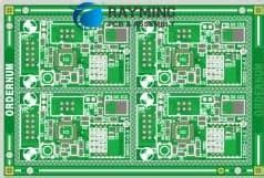
What is PCB Panelization?
PCB panelization is the process of grouping multiple printed circuit board (PCB) designs into a single panel layout for manufacturing. By combining smaller PCBs into a larger panel, you can optimize the use of materials, reduce manufacturing costs, and increase production efficiency.
Panelization is typically done using computer-aided manufacturing (CAM) software, which allows you to arrange your PCB designs, add tooling features, and generate the necessary files for fabrication.
Benefits of PCB Panelization
- Reduced manufacturing costs by optimizing material usage
- Increased production efficiency by fabricating multiple PCBs simultaneously
- Improved handling and assembly of smaller PCBs
- Simplified testing and quality control
PCB Panelization Techniques
There are several techniques used for PCB panelization, each with its own advantages and considerations.
Tab Routing
Tab routing involves connecting individual PCBs with small tabs that can be easily broken after fabrication. This method is suitable for low-volume production and allows for easy separation of the individual boards.
Advantages:
– Simple and cost-effective for low-volume production
– Easy to separate individual PCBs
Disadvantages:
– Not suitable for high-volume production
– Tabs can leave rough edges on the PCBs after separation
V-Scoring
V-scoring uses a special cutting tool to create V-shaped grooves between the individual PCBs on the panel. This technique allows for clean and easy separation of the boards without leaving rough edges.
Advantages:
– Clean and easy separation of individual PCBs
– Suitable for high-volume production
Disadvantages:
– Requires special tooling for V-scoring
– May weaken the panel during handling and assembly
Mouse Bites
Mouse bites are small, perforated holes placed between the individual PCBs on the panel. These holes allow for easy separation of the boards by simply breaking them apart along the perforations.
Advantages:
– Easy to separate individual PCBs
– Suitable for low to medium-volume production
Disadvantages:
– Can leave rough edges on the PCBs after separation
– May weaken the panel during handling and assembly
| Technique | Advantages | Disadvantages |
|---|---|---|
| Tab Routing | – Simple and cost-effective for low-volume production – Easy to separate individual PCBs |
– Not suitable for high-volume production – Tabs can leave rough edges on the PCBs after separation |
| V-Scoring | – Clean and easy separation of individual PCBs – Suitable for high-volume production |
– Requires special tooling for V-scoring – May weaken the panel during handling and assembly |
| Mouse Bites | – Easy to separate individual PCBs – Suitable for low to medium-volume production |
– Can leave rough edges on the PCBs after separation – May weaken the panel during handling and assembly |

Panelization Design Considerations
When designing your PCB panel, there are several factors to consider to ensure optimal manufacturability and assembly.
Panel Size and Material
Choose a panel size that maximizes material utilization while considering your PCB dimensions and the capabilities of your manufacturing partner. Common panel sizes include:
- 18″ x 24″ (457 mm x 610 mm)
- 21″ x 24″ (533 mm x 610 mm)
- 16″ x 18″ (406 mm x 457 mm)
The most common material for PCB panels is FR-4, a fiberglass-reinforced epoxy laminate. Other materials, such as aluminum or flexible substrates, may be used for specific applications.
Spacing and Clearance
Ensure adequate spacing between individual PCBs on the panel to allow for proper tooling and separation. A minimum spacing of 3-5 mm is typically recommended, but consult with your manufacturing partner for specific guidelines.
Also, consider the clearance required for any components that may overhang the edges of the individual PCBs. Adequate clearance will prevent damage to components during panelization and assembly.
Fiducial Marks
Fiducial marks are small, precise reference points used by automated assembly equipment to align and position the PCB panel accurately. Include at least three fiducial marks on your panel design, typically located near the corners and center of the panel.
Tooling Holes and Rails
Tooling holes and rails are used to secure the PCB panel during fabrication and assembly. Include tooling holes and rails in your panel design according to your manufacturing partner’s specifications.
| Design Consideration | Recommendation |
|---|---|
| Panel Size | – 18″ x 24″ (457 mm x 610 mm) – 21″ x 24″ (533 mm x 610 mm) – 16″ x 18″ (406 mm x 457 mm) |
| Material | FR-4 (fiberglass-reinforced epoxy laminate) |
| Spacing and Clearance | Minimum 3-5 mm between individual PCBs |
| Fiducial Marks | At least three, located near corners and center of the panel |
| Tooling Holes and Rails | According to manufacturing partner’s specifications |

CAM Software for PCB Panelization
Several CAM software options are available for PCB panelization, each with its own features and capabilities.
Altium Designer
Altium Designer is a comprehensive PCB design and manufacturing software that includes powerful panelization tools. Its intuitive interface and extensive library of components make it a popular choice among PCB designers.
Features:
– Automatic and manual panelization options
– Support for various panelization techniques, including tab routing and V-scoring
– 3D visualization of the panelized design
KiCAD
KiCAD is a free, open-source PCB design software that offers panelization capabilities through its PcbNew module. While it may have a steeper learning curve compared to commercial software, KiCAD provides a cost-effective solution for PCB panelization.
Features:
– Manual panelization tools
– Support for tab routing and mouse bites
– Integration with the KiCAD PCB design workflow
Mentor Graphics Xpedition
Mentor Graphics Xpedition is a high-end PCB design and manufacturing software suite that includes advanced panelization features. Its powerful tools and extensive automation capabilities make it well-suited for complex, high-density PCB designs.
Features:
– Automatic and manual panelization options
– Support for various panelization techniques, including tab routing and V-scoring
– Built-in design rule checks (DRC) for panelization
| Software | Features |
|---|---|
| Altium Designer | – Automatic and manual panelization options – Support for various panelization techniques – 3D visualization of the panelized design |
| KiCAD | – Manual panelization tools – Support for tab routing and mouse bites – Integration with the KiCAD PCB design workflow |
| Mentor Graphics Xpedition | – Automatic and manual panelization options – Support for various panelization techniques – Built-in design rule checks (DRC) for panelization |

Panelization Workflow
The PCB panelization workflow typically involves the following steps:
- Design individual PCBs using your preferred PCB design software
- Export the PCB designs in a format compatible with your chosen CAM software (e.g., Gerber, ODB++)
- Import the PCB designs into your CAM software
- Arrange the individual PCBs on the panel, considering spacing, clearance, and tooling requirements
- Add fiducial marks, tooling holes, and rails to the panel design
- Apply your preferred panelization technique (e.g., tab routing, V-scoring, or mouse bites)
- Generate the necessary manufacturing files (e.g., Gerber, drill files) for the panelized design
- Send the manufacturing files to your PCB fabrication partner
Best Practices for PCB Panelization
To ensure successful PCB panelization and manufacturing, consider the following best practices:
- Communicate with your PCB fabrication partner early in the design process to discuss panelization requirements and guidelines
- Keep your PCB designs as uniform as possible to simplify panelization and optimize material usage
- Use a consistent grid system for placing components and routing traces to facilitate panelization
- Minimize the use of irregular board shapes and cutouts to simplify panelization and reduce manufacturing costs
- Test your panelized design using your CAM software’s built-in design rule checks (DRC) to identify and resolve any issues before manufacturing
FAQ
1. What is the minimum spacing between individual PCBs on a panel?
A minimum spacing of 3-5 mm between individual PCBs is typically recommended, but it’s essential to consult with your PCB fabrication partner for specific guidelines, as requirements may vary depending on the manufacturing process and equipment used.
2. Can I mix different PCB designs on the same panel?
Yes, you can mix different PCB designs on the same panel, as long as they share similar characteristics, such as board thickness, copper weight, and surface finish. However, mixing designs may increase the complexity of the panelization process and could lead to higher manufacturing costs.
3. What is the most cost-effective panelization technique?
The most cost-effective panelization technique depends on factors such as the volume of production, the size and complexity of the PCBs, and the capabilities of your manufacturing partner. Tab routing is often the simplest and most cost-effective method for low-volume production, while V-scoring may be more suitable for high-volume production.
4. How do I choose the right panel size for my PCB designs?
When choosing a panel size, consider factors such as the dimensions of your individual PCBs, the number of PCBs you need to produce, and the capabilities of your manufacturing partner. Common panel sizes include 18″ x 24″, 21″ x 24″, and 16″ x 18″. Aim to maximize material utilization while ensuring adequate spacing and clearance between the individual PCBs.
5. Can I panelize flexible PCBs?
Yes, flexible PCBs can be panelized, but the process may require special considerations and techniques compared to rigid PCBs. Consult with your PCB fabrication partner to discuss the specific requirements and guidelines for panelizing flexible PCBs, as they may need to use different materials, tooling, and separation methods.
Conclusion
PCB panelization is a crucial step in the PCB manufacturing process, allowing for increased production efficiency, reduced costs, and improved handling of smaller PCBs. By understanding the various panelization techniques, design considerations, and best practices, you can optimize your PCB designs for successful panelization and manufacturing.
When working on PCB panelization, it’s essential to collaborate closely with your PCB fabrication partner to ensure that your designs meet their specific requirements and guidelines. By using the appropriate CAM software and following a structured panelization workflow, you can streamline the process and achieve high-quality results.
As you continue to design and panelize PCBs, stay informed about the latest industry trends, technologies, and best practices to continuously improve your skills and deliver successful projects.
Leave a Reply