Introduction to Copper-Based Printed Circuit Boards
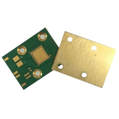
A printed circuit board, or PCB, is the foundation of nearly all modern electronic devices. PCBs provide mechanical support and electrical connections for electronic components using conductive pathways, tracks, or signal traces etched from copper sheets laminated onto a non-conductive substrate. One of the most common types is the copper-based PCB, where copper is the primary conductive material used for the circuit traces.
Copper-based PCBs offer several advantages that make them a popular choice for a wide range of applications, from consumer electronics to industrial equipment and aerospace systems. This article will delve into the basics of copper-based PCBs, their manufacturing process, advantages, and applications.
Key Characteristics of Copper Used in PCBs
Copper is the most widely used conductive material for PCBs due to its excellent electrical and thermal properties. Some of the key characteristics that make copper an ideal choice for PCBs include:
- High electrical conductivity
- Good thermal conductivity
- Excellent solderability
- Resistance to corrosion
- Cost-effectiveness compared to other conductive materials
Copper used in PCBs typically has a purity level of 99.9% or higher to ensure optimal performance and reliability.
Manufacturing Process of Copper-Based PCBs
The manufacturing process of copper-based PCBs involves several steps, each of which is critical to ensuring the quality and functionality of the final product.
1. PCB Design and Layout
The first step in manufacturing a copper-based PCB is designing the circuit layout using specialized software. The design includes the placement of components, routing of traces, and creation of copper layers. The design files are then used to generate photomasks for the subsequent fabrication steps.
2. Substrate Preparation
The substrate, typically made of FR-4 (a glass-reinforced epoxy laminate), is cut to the required size and shape. Copper foils are then laminated onto one or both sides of the substrate using heat and pressure. The thickness of the copper foil can vary depending on the application, with common thicknesses ranging from 0.5 oz to 2 oz per square foot.
3. Photoresist Application and Exposure
A photoresist layer is applied onto the copper-clad substrate. The photoresist is a light-sensitive material that hardens when exposed to ultraviolet (UV) light. The photomask containing the circuit layout is placed on top of the photoresist, and the assembly is exposed to UV light. The areas of the photoresist not covered by the photomask harden, while the unexposed areas remain soluble.
4. Developing and Etching
The unexposed photoresist is removed using a developer solution, revealing the underlying copper layer. The PCB is then subjected to an etching process, where the exposed copper is removed using a chemical etchant, typically ferric chloride or ammonium persulfate. The hardened photoresist protects the desired copper traces during etching.
5. Photoresist Removal and Inspection
After etching, the remaining photoresist is stripped off, leaving only the copper traces on the substrate. The PCB undergoes an inspection to ensure that the traces are correctly formed and there are no defects.
6. Drilling and Plating
Holes are drilled through the PCB to accommodate through-hole components and vias. The holes are then plated with copper to establish electrical connections between layers.
7. Solder Mask Application and Silkscreen
A solder mask, usually green in color, is applied to the PCB to protect the copper traces from oxidation and prevent solder bridges during the soldering process. The solder mask also helps to insulate the traces. A silkscreen layer is then added to provide text and symbols for component placement and identification.
8. Surface Finish and Final Inspection
A surface finish, such as HASL (Hot Air Solder Leveling), ENIG (Electroless Nickel Immersion Gold), or OSP (Organic Solderability Preservative), is applied to the exposed copper pads to enhance solderability and protect the copper from oxidation. The PCB undergoes a final inspection to ensure it meets the required specifications before being packaged and shipped.

Advantages of Copper-Based PCBs
Copper-based PCBs offer several advantages that contribute to their widespread use in the electronics industry.
1. Excellent Electrical Conductivity
Copper has a high electrical conductivity, second only to silver among metals. This property ensures efficient and reliable signal transmission, reducing power losses and heat generation.
2. Good Thermal Conductivity
Copper’s good thermal conductivity helps to dissipate heat generated by electronic components, preventing overheating and improving the overall reliability of the device.
3. Excellent Solderability
Copper provides excellent solderability, allowing for strong and reliable solder joints between components and the PCB.
4. Cost-Effectiveness
Copper is more cost-effective compared to other highly conductive materials like silver or gold, making it an economical choice for large-scale PCB production.

Applications of Copper-Based PCBs
Copper-based PCBs find applications in a wide range of industries and devices, including:
- Consumer electronics (smartphones, laptops, televisions, etc.)
- Automotive electronics (engine control units, infotainment systems, etc.)
- Industrial equipment (control systems, power supplies, etc.)
- Medical devices (diagnostic equipment, patient monitors, etc.)
- Aerospace and defense systems (avionics, communication systems, etc.)
- Internet of Things (IoT) devices (sensors, smart home appliances, wearables, etc.)
The versatility and reliability of copper-based PCBs make them an essential component in the ever-expanding world of electronics.

Copper Thickness and Trace Width Considerations
When designing copper-based PCBs, it is essential to consider the thickness of the copper layer and the width of the traces. These factors influence the current-carrying capacity, signal integrity, and manufacturability of the PCB.
Copper Thickness
The thickness of the copper layer is typically expressed in ounces per square foot (oz/ft²). Common copper thicknesses used in PCBs include:
| Copper Weight (oz/ft²) | Nominal Thickness (mm) | Typical Applications |
|---|---|---|
| 0.5 | 0.017 | Low-power, high-density designs |
| 1 | 0.034 | General-purpose applications |
| 2 | 0.068 | High-current, power electronics |
Thicker copper layers can carry more current and provide better heat dissipation but may increase the cost and complexity of the manufacturing process.
Trace Width
The width of the copper traces determines their current-carrying capacity and influences signal integrity. Narrower traces allow for higher component density but have lower current-carrying capacity and are more susceptible to signal integrity issues. Wider traces can carry more current and provide better signal integrity but may increase the size of the PCB.
When selecting trace widths, designers must consider factors such as:
- Current requirements of the components
- Signal frequency and rise/fall times
- PCB manufacturing capabilities
- PCB size constraints
Designers can use online calculators or design software to determine the appropriate trace widths based on the specific requirements of their project.
Copper-Based PCBs vs. Other Materials
While copper is the most common conductive material used in PCBs, there are other materials that may be used in specific applications.
Aluminum PCBs
Aluminum PCBs use aluminum as the conductive material instead of copper. They offer some advantages, such as better thermal conductivity and lower weight, making them suitable for applications that require heat dissipation or weight reduction. However, aluminum has lower electrical conductivity compared to copper and is more difficult to solder, limiting its widespread use.
Silver-Based PCBs
Silver has the highest electrical conductivity among metals, making it an attractive option for high-frequency and low-loss applications. However, silver is significantly more expensive than copper and is more susceptible to oxidation, which can lead to signal degradation over time. Silver-based PCBs are typically used in specialized applications where the benefits outweigh the costs.
FAQ
1. What is the difference between copper-clad and copper-based PCBs?
Copper-clad PCBs refer to the substrate material with a layer of copper foil laminated onto one or both sides before the etching process. Copper-based PCBs, on the other hand, refer to the completed PCB with copper traces after the etching and fabrication process.
2. Can copper-based PCBs be used for high-frequency applications?
Yes, copper-based PCBs can be used for high-frequency applications. However, designers must consider factors such as trace width, substrate material, and copper thickness to ensure optimal signal integrity and minimize losses at high frequencies.
3. How does the copper thickness affect the current-carrying capacity of a PCB?
Thicker copper layers can carry more current than thinner layers. Doubling the copper thickness allows the trace to carry twice as much current while maintaining the same temperature rise. However, thicker copper layers also increase the weight and cost of the PCB.
4. What is the purpose of the solder mask on a copper-based PCB?
The solder mask serves two main purposes on a copper-based PCB. First, it protects the copper traces from oxidation and damage during the soldering process and throughout the life of the PCB. Second, it helps to insulate the traces, preventing short circuits and improving the overall reliability of the PCB.
5. Can copper-based PCBs be recycled?
Yes, copper-based PCBs can be recycled. The recycling process involves separating the copper and other metals from the non-metallic components using various techniques, such as mechanical shredding, chemical processing, and electrolysis. Recycling copper-based PCBs helps to conserve resources, reduce waste, and minimize the environmental impact of electronic waste.
Conclusion
Copper-based PCBs are the backbone of modern electronics, offering excellent electrical and thermal properties, cost-effectiveness, and versatility. Understanding the manufacturing process, advantages, and applications of copper-based PCBs is essential for designers, engineers, and anyone involved in the electronics industry.
As technology advances and the demand for more complex and compact electronic devices grows, copper-based PCBs will continue to play a crucial role in enabling these developments. By considering factors such as copper thickness, trace width, and substrate material, designers can optimize the performance and reliability of their copper-based PCBs for a wide range of applications.
Leave a Reply