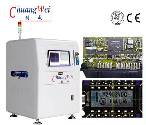
Introduction to AOI in PCB Manufacturing
Automated Optical Inspection (AOI) is a crucial technology used in the manufacturing process of Printed Circuit Boards (PCBs). AOI systems are designed to detect and identify defects or irregularities on the surface of PCBs, ensuring the quality and reliability of the final product. In the fast-paced and highly competitive electronics industry, AOI has become an essential tool for manufacturers to maintain high standards and meet customer expectations.
The Importance of Quality Control in PCB Manufacturing
PCBs are the backbone of modern electronic devices, connecting and supporting various components to enable their functionality. As these devices become increasingly complex and miniaturized, the demand for high-quality, defect-free PCBs has never been greater. Even the smallest defect or irregularity on a PCB can lead to malfunctions, reduced performance, or complete failure of the end product. This can result in costly repairs, product recalls, and damage to a manufacturer’s reputation.
To mitigate these risks and ensure the consistent production of high-quality PCBs, manufacturers employ various quality control measures throughout the manufacturing process. AOI is one of the most effective and widely used methods for detecting and preventing defects in PCBs.
The Evolution of AOI Technology
AOI technology has undergone significant advancements since its introduction in the 1980s. Early AOI systems relied on simple image comparison techniques, comparing the captured image of a PCB to a reference image of a known good board. While these systems were capable of detecting major defects, they lacked the precision and flexibility needed to keep up with the increasing complexity of PCBs.
As PCB designs became more intricate and components more miniaturized, AOI systems evolved to incorporate more sophisticated imaging technologies and advanced algorithms. Modern AOI systems use high-resolution cameras, multiple lighting angles, and powerful image processing software to capture and analyze detailed images of PCBs. These advancements have greatly improved the accuracy and speed of defect detection, enabling manufacturers to identify even the smallest irregularities with high precision.
How AOI Systems Work
The Basic Components of an AOI System
A typical AOI system consists of several key components that work together to capture, process, and analyze images of PCBs:
-
Imaging System: This includes high-resolution cameras, lenses, and lighting equipment that capture detailed images of the PCB surface. AOI systems often employ multiple cameras and lighting angles to ensure comprehensive coverage and minimize shadow effects.
-
Transport Mechanism: A conveyor system or robotic arm moves the PCB through the imaging area, ensuring precise positioning and alignment for consistent image capture.
-
Image Processing Hardware: Powerful computers and specialized hardware accelerate the image processing and analysis tasks, enabling real-time defect detection.
-
Software: Advanced algorithms and machine learning techniques are used to analyze the captured images, comparing them to a reference model or CAD data to identify defects and irregularities.
-
User Interface: A user-friendly interface allows operators to monitor the inspection process, review detected defects, and adjust system settings as needed.
The AOI Inspection Process
The AOI inspection process typically involves the following steps:
-
PCB Loading: The PCB is placed on the transport mechanism, which moves it into the imaging area.
-
Image Capture: As the PCB moves through the imaging area, the cameras capture high-resolution images of the surface from various angles and under different lighting conditions.
-
Image Processing: The captured images are processed and analyzed by the system’s software, which applies various algorithms and techniques to identify defects and irregularities.
-
Defect Detection: The system compares the processed images to a reference model or CAD data, identifying any deVIAtions or anomalies that indicate the presence of a defect.
-
Defect Classification: Detected defects are classified according to their type, severity, and location on the PCB. Common defect types include solder bridges, open circuits, short circuits, and component misalignment.
-
Reporting: The system generates a detailed report of the inspection results, including the location and type of each detected defect. This information is used by operators to make informed decisions about the acceptability of the PCB and to initiate necessary corrective actions.
Advantages of AOI over Manual Inspection
AOI offers several key advantages over traditional manual inspection methods:
-
Speed: AOI systems can inspect PCBs at a much faster rate than human inspectors, enabling higher throughput and shorter production times.
-
Consistency: AOI systems apply the same inspection criteria to every PCB, ensuring consistent and reliable defect detection regardless of operator skill or fatigue.
-
Accuracy: Advanced imaging technologies and algorithms enable AOI systems to detect even the smallest defects with high precision, reducing the risk of false positives or false negatives.
-
Traceability: AOI systems generate detailed reports and store inspection data, providing a comprehensive record of the quality control process for each PCB.
-
Cost-effectiveness: By automating the inspection process and catching defects early in the manufacturing cycle, AOI helps reduce costs associated with manual labor, rework, and scrap.

Types of AOI Systems
There are several types of AOI systems used in PCB manufacturing, each with its own strengths and applications:
2D AOI Systems
2D AOI systems capture and analyze two-dimensional images of the PCB surface. These systems are well-suited for inspecting features such as solder joints, component placement, and circuit patterns. 2D AOI is widely used for its simplicity, speed, and cost-effectiveness.
3D AOI Systems
3D AOI systems use advanced imaging techniques, such as structured light or laser scanning, to capture three-dimensional data of the PCB surface. This enables the detection of defects related to component height, coplanarity, and solder joint volume. 3D AOI is particularly useful for inspecting complex assemblies and identifying defects that may be difficult to detect using 2D imaging alone.
Inline AOI Systems
Inline AOI systems are integrated directly into the production line, inspecting PCBs immediately after the solder paste printing, component placement, or soldering processes. This allows for real-time defect detection and correction, minimizing the risk of defective boards proceeding to subsequent stages of the manufacturing process.
Offline AOI Systems
Offline AOI systems are standalone units that inspect PCBs after they have been removed from the production line. These systems offer greater flexibility and can be used for batch inspection or as a complement to inline AOI. Offline AOI is often used for final quality control checks or for inspecting PCBs that require more extensive testing.

Challenges and Limitations of AOI
While AOI is a powerful tool for detecting defects in PCBs, it is not without its challenges and limitations:
False Positives and False Negatives
AOI systems can occasionally generate false positives (identifying a defect where none exists) or false negatives (failing to detect a real defect). These errors can lead to unnecessary rework or the release of defective products. To minimize these risks, manufacturers must carefully calibrate and optimize their AOI systems, as well as implement secondary inspection methods to verify the results.
Limited Depth Perception
2D AOI systems may struggle to detect defects that are hidden or obscured by other components, as they lack the depth perception provided by 3D imaging. This can be particularly challenging for inspecting high-density assemblies or boards with tall components.
Reflective Surfaces
Highly reflective surfaces, such as those found on certain components or solder joints, can create glare and reflection that interfere with the AOI system’s ability to capture clear images. This can lead to reduced defect detection accuracy. To mitigate this issue, manufacturers may need to adjust lighting conditions or use specialized imaging techniques.
Keeping Pace with Technological Advancements
As PCB designs continue to evolve and become more complex, AOI systems must adapt to keep pace with these changes. This requires continuous investment in research and development to improve imaging technologies, algorithms, and data processing capabilities. Manufacturers must carefully balance the costs and benefits of upgrading their AOI systems to ensure they remain competitive and meet the changing demands of the industry.

Best Practices for Implementing AOI in PCB Manufacturing
To mAXImize the benefits of AOI and ensure its effective implementation, manufacturers should consider the following best practices:
Selecting the Right AOI System
Choosing the appropriate AOI system depends on various factors, such as the complexity of the PCBs being manufactured, the production volume, and the specific defects that need to be detected. Manufacturers should carefully evaluate their requirements and consult with AOI vendors to select a system that best meets their needs.
Proper Training and Operator Skills
While AOI systems automate much of the inspection process, human operators still play a crucial role in setting up, monitoring, and maintaining the equipment. Proper training is essential to ensure that operators understand the capabilities and limitations of the AOI system, as well as how to interpret and act upon the inspection results.
Regular Calibration and Maintenance
To ensure consistent and reliable performance, AOI systems must be regularly calibrated and maintained. This includes cleaning lenses and lighting equipment, replacing worn or damaged components, and updating software as needed. Manufacturers should establish a routine maintenance schedule and train operators to perform basic upkeep tasks.
Integration with Other Quality Control Methods
AOI should not be viewed as a standalone solution but rather as part of a comprehensive quality control strategy. Manufacturers should integrate AOI with other inspection methods, such as X-ray inspection or functional testing, to provide a more complete picture of PCB quality. This multi-layered approach helps to catch defects that may be missed by a single inspection method and ensures the highest possible level of quality assurance.
Continuous Improvement and Data Analysis
The data generated by AOI systems can provide valuable insights into the manufacturing process, helping to identify patterns or trends in defect occurrence. Manufacturers should regularly analyze this data to identify opportunities for process improvement, such as optimizing solder paste application or adjusting component placement parameters. By continuously monitoring and refining the manufacturing process, manufacturers can reduce defect rates and improve overall product quality.
Frequently Asked Questions (FAQ)
-
What are the most common defects detected by AOI systems?
Some of the most common defects detected by AOI systems include solder bridges, open circuits, short circuits, component misalignment, and missing or incorrect components. -
Can AOI systems detect defects that are hidden under components?
2D AOI systems may struggle to detect defects that are hidden under components, as they lack the depth perception provided by 3D imaging. In these cases, manufacturers may need to use complementary inspection methods, such as X-ray inspection, to identify hidden defects. -
How fast can AOI systems inspect PCBs?
The speed of AOI inspection depends on various factors, such as the size and complexity of the PCB, the resolution of the imaging system, and the specific defects being detected. However, AOI systems can generally inspect PCBs at a much faster rate than manual inspection, with some systems capable of inspecting thousands of components per minute. -
Are AOI systems capable of inspecting both sides of a PCB?
Yes, many AOI systems are designed to inspect both sides of a PCB, either by using multiple cameras or by flipping the board during the inspection process. This ensures comprehensive coverage and helps to detect defects that may be present on either side of the PCB. -
How do manufacturers ensure the accuracy of AOI systems?
To ensure the accuracy of AOI systems, manufacturers employ various techniques, such as regular calibration, using high-quality reference images or CAD data, and optimizing lighting and imaging parameters. Additionally, manufacturers often use secondary inspection methods to verify the results of AOI and catch any defects that may have been missed.
Conclusion
Automated Optical Inspection (AOI) has become an indispensable tool in the PCB manufacturing process, enabling manufacturers to detect and prevent defects with high speed, accuracy, and consistency. By implementing AOI systems and following best practices for their use and maintenance, manufacturers can significantly improve the quality and reliability of their products, reduce costs associated with rework and scrap, and enhance their competitiveness in the market.
As PCB designs continue to evolve and become more complex, the role of AOI in ensuring product quality will only become more critical. Manufacturers that invest in advanced AOI technologies and integrate them into their overall quality control strategy will be well-positioned to meet the challenges of the future and deliver the high-quality products that customers demand.
Leave a Reply