Introduction to Automated Optical Inspection (AOI)
Automated Optical Inspection (AOI) is a critical process in the manufacturing of printed circuit boards (PCBs). It involves using specialized cameras and image processing software to automatically inspect PCBs for defects, ensuring the quality and reliability of the final product. AOI systems are designed to detect a wide range of defects, including missing components, incorrect component placement, solder defects, and circuit pattern errors.
The use of AOI in PCB manufacturing has become increasingly important as PCBs have become more complex and miniaturized. Manual inspection of PCBs is time-consuming, error-prone, and often impractical for high-volume production. AOI systems, on the other hand, can inspect PCBs quickly and accurately, identifying defects that may be missed by human inspectors.
How Does Automated Optical Inspection (AOI) Work?
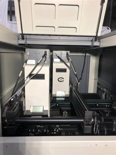
AOI systems typically consist of three main components: a camera system, lighting system, and image processing software. The camera system captures high-resolution images of the PCB from multiple angles, while the lighting system provides consistent illumination to enhance the visibility of defects. The image processing software then analyzes the captured images, comparing them to a reference image of a known good PCB to identify any discrepancies.
The AOI inspection process can be broken down into several steps:
- Image Acquisition: The PCB is placed in the AOI machine, and the camera system captures high-resolution images of the board from various angles.
- Image Preprocessing: The captured images are preprocessed to enhance their quality and remove any noise or artifacts that may interfere with the inspection process.
- Image Analysis: The preprocessed images are analyzed by the image processing software, which compares them to a reference image of a known good PCB. The software uses advanced algorithms to detect any discrepancies between the two images, such as missing components, incorrect component placement, or solder defects.
- Defect Classification: If a discrepancy is detected, the software classifies it according to predefined defect categories, such as missing component, misaligned component, or solder bridge.
- Reporting: The AOI system generates a report detailing any defects found during the inspection process, including their location, type, and severity. This report can be used by operators to repair or rework the PCB as needed.

Benefits of Automated Optical Inspection (AOI) in PCB Manufacturing
The use of AOI in PCB manufacturing offers several significant benefits, including:
- Improved Quality: AOI systems can detect a wide range of defects that may be missed by human inspectors, ensuring that only high-quality PCBs are shipped to customers.
- Increased Efficiency: AOI systems can inspect PCBs much faster than human inspectors, allowing manufacturers to increase their production throughput without sacrificing quality.
- Reduced Costs: By catching defects early in the manufacturing process, AOI systems can help manufacturers avoid the costs associated with rework, scrap, and warranty claims.
- Consistent Inspection: AOI systems provide consistent and repeatable inspection results, eliminating the variability that can occur with manual inspection.
- Traceability: AOI systems generate detailed inspection reports that can be used to track and trace defects, helping manufacturers identify and address root causes of quality issues.

Types of Defects Detected by Automated Optical Inspection (AOI)
AOI systems are designed to detect a wide range of defects that can occur during the PCB manufacturing process. Some of the most common types of defects detected by AOI include:
| Defect Type | Description |
|---|---|
| Missing Component | A component is missing from its designated location on the PCB. |
| Misaligned Component | A component is not placed accurately on the PCB, either in terms of position or orientation. |
| Incorrect Component | The wrong component is placed on the PCB, either in terms of value, package size, or polarity. |
| Solder Defects | Defects related to the solder joints, such as insufficient solder, excess solder, solder bridges, or cold solder joints. |
| Circuit Pattern Defects | Defects in the copper traces or pads on the PCB, such as open circuits, short circuits, or incorrect trace width or spacing. |
| Surface Defects | Defects on the surface of the PCB, such as scratches, dents, or contamination. |

Limitations of Automated Optical Inspection (AOI)
While AOI is a powerful tool for detecting defects in PCBs, it does have some limitations:
- False Positives and False Negatives: AOI systems are not perfect and can sometimes generate false positives (identifying a defect that is not actually present) or false negatives (failing to identify a defect that is present). These errors can be caused by factors such as poor image quality, incorrect reference data, or limitations in the image processing algorithms.
- Limited Depth Perception: AOI systems rely on 2D images to detect defects, which can limit their ability to detect defects that are hidden or obscured by other components or features on the PCB.
- Inability to Detect Functional Defects: AOI systems can only detect visible defects on the surface of the PCB. They cannot detect functional defects, such as incorrect component values or incorrect circuit behavior, which may require additional testing methods.
- Setup and Programming: AOI systems require significant setup and programming to ensure that they are properly configured to detect the specific defects that can occur on a particular PCB design. This setup process can be time-consuming and requires skilled personnel.
Automated Optical Inspection (AOI) vs. Manual Inspection
While AOI has many advantages over manual inspection, there are still some situations where manual inspection may be preferred or required. The following table compares the key differences between AOI and manual inspection:
| Factor | AOI | Manual Inspection |
|---|---|---|
| Speed | High-speed, can inspect hundreds of PCBs per hour | Slow, limited by human visual acuity and attention span |
| Accuracy | Consistent and repeatable, can detect small defects | Variable, depends on the skill and experience of the inspector |
| Cost | High initial investment, but lower long-term costs | Low initial investment, but higher long-term labor costs |
| Flexibility | Limited to predefined defect categories and inspection algorithms | Can adapt to new or unexpected defect types |
| Subjectivity | Objective, based on predefined criteria and algorithms | Subjective, can be influenced by human factors such as fatigue or bias |
In practice, many PCB manufacturers use a combination of AOI and manual inspection to ensure the highest level of quality control. AOI is often used as a first-line inspection method to quickly identify and remove PCBs with obvious defects, while manual inspection is used to verify the results of AOI and to inspect PCBs with more complex or unusual defects.
Integration of Automated Optical Inspection (AOI) into the PCB Manufacturing Process
To maximize the benefits of AOI, it is important to integrate it effectively into the overall PCB manufacturing process. This typically involves the following steps:
- Design for Manufacturability (DFM): The PCB design should be optimized for manufacturability, taking into account factors such as component placement, solder pad size and shape, and circuit trace routing. This can help to minimize the occurrence of defects and improve the effectiveness of AOI.
- Process Control: The PCB manufacturing process should be carefully controlled to ensure consistent quality and minimize the occurrence of defects. This may involve the use of statistical process control (SPC) methods to monitor and adjust process parameters such as solder paste deposition, component placement, and reflow soldering.
- AOI Programming: The AOI system should be programmed with the appropriate reference data and inspection algorithms for each PCB design. This may involve creating a “golden board” or reference PCB that represents the ideal state of the board, and using this to train the AOI system to recognize defects.
- Verification and Validation: The results of AOI should be verified and validated through additional testing methods, such as manual inspection, electrical testing, or Functional Testing. This can help to identify any false positives or false negatives generated by the AOI system and ensure that the final product meets all quality and performance requirements.
- Continuous Improvement: The data generated by AOI should be used to drive continuous improvement efforts in the PCB manufacturing process. This may involve identifying and addressing the root causes of recurring defects, optimizing process parameters, or improving the design of the PCB itself.
Frequently Asked Questions (FAQ)
- What is the difference between 2D and 3D AOI?
2D AOI uses a single camera to capture a 2D image of the PCB, while 3D AOI uses multiple cameras or laser sensors to capture a 3D image of the PCB. 3D AOI can provide more detailed information about the height and volume of components and solder joints, but is generally more expensive and slower than 2D AOI. - Can AOI detect all types of defects?
No, AOI is primarily designed to detect visible defects on the surface of the PCB, such as missing components, misaligned components, and solder defects. It cannot detect hidden or functional defects, such as incorrect component values or incorrect circuit behavior. - How much does an AOI system cost?
The cost of an AOI system can vary widely depending on factors such as the size and complexity of the PCBs being inspected, the speed and accuracy requirements, and the level of automation and integration with other manufacturing systems. Entry-level AOI systems may cost around $50,000, while high-end systems can cost over $500,000. - Can AOI be used for flexible or non-planar PCBs?
Yes, some AOI systems are specifically designed for inspecting flexible or non-planar PCBs, such as those used in smartphones or wearable devices. These systems may use specialized cameras or lighting techniques to accommodate the unique challenges of inspecting non-flat surfaces. - How long does it take to program an AOI system for a new PCB design?
The time required to program an AOI system for a new PCB design can vary depending on the complexity of the board and the experience of the programming team. A simple PCB may take a few hours to program, while a complex PCB with many components and fine-pitch features may take several days or even weeks to program and validate.
Conclusion
Automated Optical Inspection (AOI) is a critical technology for ensuring the quality and reliability of printed circuit boards (PCBs) in modern electronics manufacturing. By using advanced camera systems, lighting, and image processing software, AOI can quickly and accurately detect a wide range of defects that may be missed by human inspectors, such as missing components, misaligned components, and solder defects.
While AOI has some limitations, such as the inability to detect hidden or functional defects, it offers significant benefits in terms of improved quality, increased efficiency, reduced costs, and consistent inspection results. To maximize these benefits, it is important to integrate AOI effectively into the overall PCB manufacturing process, including design for manufacturability, process control, AOI programming, verification and validation, and continuous improvement efforts.
As PCBs continue to become more complex and miniaturized, the use of AOI is likely to become even more important in the future. By staying up-to-date with the latest AOI technologies and best practices, PCB manufacturers can ensure that they are delivering the highest quality products to their customers while minimizing costs and maximizing efficiency.
Leave a Reply