Introduction to SMT-LaserStencil
Surface Mount Technology (SMT) has revolutionized the electronics manufacturing industry by enabling the production of smaller, lighter, and more efficient electronic devices. One of the critical components in the SMT assembly process is the stencil, which is used to apply solder paste onto the printed circuit board (PCB) before placing the components. SMT Stencils can be made using various methods, but laser-cut stencils have gained popularity due to their precision, durability, and quick turnaround times.
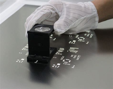
What is an SMT Stencil?
An SMT stencil is a thin sheet of metal, typically stainless steel, with apertures or openings that correspond to the pads on a PCB. The stencil is placed over the PCB, and solder paste is applied using a squeegee, forcing the paste through the openings and onto the pads. The stencil ensures that the correct amount of solder paste is deposited on each pad, which is crucial for proper component placement and soldering.
Advantages of Using SMT Stencils
Using SMT stencils offers several advantages in the electronics manufacturing process:
- Precision: SMT stencils ensure accurate and consistent solder paste deposition, resulting in fewer assembly defects and higher yields.
- Efficiency: Stencils allow for the rapid application of solder paste to multiple PCBs, increasing production throughput.
- Repeatability: Stencils provide a repeatable process, ensuring consistent results across different production runs.
- Versatility: SMT stencils can be used with various solder paste types and can accommodate a wide range of component sizes and pitches.
Laser-Cut SMT Stencils
Laser-cut SMT stencils, also known as laser stencils, are created using high-precision laser cutting machines. These machines use focused laser beams to cut the stencil material, creating clean and accurate apertures. Laser stencils offer several advantages over traditional chemically-etched or electroformed stencils.
Advantages of Laser Stencils
- High Precision: Laser cutting machines can achieve very tight tolerances, resulting in highly accurate and consistent apertures. This precision is especially important for fine-pitch components and high-density PCB designs.
- Quick Turnaround: Laser cutting is a fast process, allowing for shorter lead times compared to chemical etching or electroforming. This is particularly beneficial for prototyping and low-volume production runs.
- Durability: Laser-cut stencils have smooth, burr-free aperture walls, which reduce wear and tear on the stencil and increase its lifespan. This also helps maintain consistent solder paste deposition over time.
- Flexibility: Laser stencils can be easily modified or updated by simply changing the CAD file and cutting a new stencil. This flexibility allows for quick design iterations and accommodates last-minute changes.
Laser Stencil Materials
Laser-cut SMT stencils are typically made from stainless steel, which offers excellent durability, stability, and resistance to corrosion. The most common stainless steel grades used for laser stencils are:
- 304 Stainless Steel: This is the most widely used material for laser stencils due to its good corrosion resistance and cost-effectiveness.
- 316 Stainless Steel: This grade offers superior corrosion resistance compared to 304 stainless steel, making it suitable for applications involving corrosive solder paste or harsh cleaning agents.
- Nickel-plated Stainless Steel: Nickel-plated stencils provide excellent wear resistance and a smooth surface finish, which helps prevent solder paste adhesion and facilitates easier cleaning.
Laser Stencil Thickness
The thickness of a laser stencil plays a crucial role in determining the amount of solder paste deposited on the PCB pads. Thicker stencils deposit more solder paste, while thinner stencils deposit less. The optimal stencil thickness depends on various factors, such as the component size, pitch, and the desired solder joint profile.
Common laser stencil thicknesses include:
| Thickness (mil) | Thickness (mm) | Typical Applications |
|---|---|---|
| 3 | 0.076 | Ultra-fine pitch components |
| 4 | 0.1016 | Fine-pitch components |
| 5 | 0.127 | Standard SMT components |
| 6 | 0.1524 | Large SMT components |
| 7 | 0.1778 | High-volume solder paste deposition |
Choosing the right stencil thickness is essential for achieving the desired solder joint profile and ensuring reliable solder connections.

Designing for Laser Stencils
When designing a PCB for use with a laser stencil, there are several guidelines to follow to ensure optimal solder paste deposition and component placement.
Aperture Design
Aperture design is critical for achieving the correct solder paste volume and preventing issues such as bridging or insufficient solder joints. Some key considerations include:
- Aperture Size: The aperture size should be slightly larger than the pad size to accommodate the solder paste volume and allow for some misalignment during stencil placement. A common rule of thumb is to add 10-20% to the pad size for the aperture size.
- Aperture Shape: The most common aperture shapes are square and rectangular, but round and oblong apertures can be used for specific components or pad geometries. The aperture shape should be chosen based on the pad shape and the desired solder joint profile.
- Aperture Wall Angle: Laser-cut stencils typically have aperture walls with a slight taper, usually between 1-5 degrees. This taper helps with solder paste release and prevents bridging between adjacent pads.
Fiducial Marks
Fiducial marks are reference points on the PCB and stencil that help align the two during the Solder paste printing process. Fiducial marks should be included in the PCB and stencil design to ensure accurate alignment and consistent solder paste deposition.
Stencil Frame Design
The stencil frame holds the stencil in place during the printing process and provides structural support. The frame design should consider the following:
- Frame Size: The frame size should be large enough to accommodate the PCB and provide sufficient space for handling and mounting.
- Mounting holes: The frame should include mounting holes that are compatible with the solder paste printer being used.
- Tensioning: The frame should provide adequate tensioning to keep the stencil flat and prevent warping or sagging during the printing process.

Solder Paste Printing Process
The solder paste printing process using a laser stencil involves several steps to ensure consistent and accurate solder paste deposition.
Stencil Alignment
The first step is to align the stencil with the PCB using the fiducial marks. This is typically done using a solder paste printer with an automated vision system that detects the fiducial marks and aligns the stencil accordingly.
Solder Paste Application
Once the stencil is aligned, solder paste is applied to the stencil using a squeegee. The squeegee is typically made of metal or rubber and is moved across the stencil at a specific speed and pressure to force the solder paste through the apertures and onto the PCB pads.
Stencil Cleaning
After solder paste application, the stencil must be cleaned to remove any excess solder paste or debris that may have accumulated on the surface or in the apertures. This can be done using various methods, such as manual cleaning with solvents or automated stencil cleaning systems.

Maintenance and Storage
Proper maintenance and storage of laser stencils are essential for ensuring consistent performance and longevity.
Cleaning
Regular cleaning of laser stencils is necessary to prevent solder paste buildup and maintain aperture accuracy. Stencils can be cleaned using various methods, such as:
- Manual Cleaning: This involves using solvents and wiping the stencil surface with a lint-free cloth or brush.
- Ultrasonic Cleaning: Ultrasonic Cleaners use high-frequency sound waves to agitate a cleaning solution, effectively removing solder paste residue from the stencil surface and apertures.
- Automated Cleaning: Automated stencil cleaning systems use a combination of solvents, brushes, and air knives to clean the stencil surface and apertures.
Storage
Proper storage of laser stencils is crucial for preventing damage and maintaining their performance. Stencils should be stored in a clean, dry environment and protected from physical damage. Some best practices for stencil storage include:
- Vertical Storage: Storing stencils vertically helps prevent warping and sagging, which can affect the accuracy of solder paste deposition.
- Protective Covers: Using protective covers or bags can help prevent dust, debris, or moisture from accumulating on the stencil surface during storage.
- Temperature and Humidity Control: Stencils should be stored in an environment with controlled temperature and humidity to prevent corrosion or warping due to environmental factors.
Frequently Asked Questions
1. What is the difference between laser stencils and chemically-etched stencils?
Laser stencils are cut using a high-precision laser cutting machine, resulting in clean, burr-free apertures with tight tolerances. Chemically-etched stencils are created using a photochemical etching process, which can result in less precise apertures and may require additional post-processing to remove burrs or rough edges.
2. How long do laser stencils last?
The lifespan of a laser stencil depends on various factors, such as the material, thickness, and usage frequency. With proper maintenance and storage, a laser stencil can typically last for several thousand prints before needing to be replaced.
3. Can laser stencils accommodate fine-pitch components?
Yes, laser stencils are well-suited for fine-pitch components due to their high precision and ability to create small, accurate apertures. Laser cutting machines can achieve aperture sizes as small as 0.1 mm, making them suitable for even the most demanding fine-pitch applications.
4. How do I choose the right stencil thickness for my application?
The optimal stencil thickness depends on factors such as the component size, pitch, and desired solder joint profile. As a general guideline, thinner stencils (3-4 mil) are used for fine-pitch components, while thicker stencils (5-7 mil) are used for larger components or higher solder paste volume requirements. It’s essential to consult with your stencil manufacturer or assembly partner to determine the best stencil thickness for your specific application.
5. Are laser stencils compatible with all solder paste types?
Laser stencils are compatible with most solder paste types, including lead-based and lead-free solder pastes. However, it’s essential to consider the solder paste’s properties, such as viscosity and particle size, when selecting a stencil thickness and aperture design to ensure optimal solder paste deposition and release.
Conclusion
Laser-cut SMT stencils have become an essential tool in the electronics manufacturing industry, offering high precision, durability, and quick turnaround times for solder paste deposition. By understanding the advantages of laser stencils, proper design guidelines, and maintenance practices, manufacturers can optimize their SMT assembly process and achieve consistent, high-quality solder joints.
As electronics continue to become smaller and more complex, the demand for precise and reliable solder paste deposition methods will only increase. Laser stencils are well-positioned to meet these challenges and will likely remain a crucial component in the SMT assembly process for years to come.
Leave a Reply