Introduction
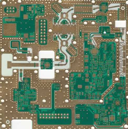
Printed circuit boards (PCBs) that operate at radio frequencies (RF) require special design considerations compared to traditional digital PCBs. Proper RF PCB design is critical for achieving desired performance in wireless systems. This article will cover key RF layout rules and best practices.
Matching Component Values
When selecting components for an RF PCB, it is important to match values precisely. Small variations in component values can greatly impact impedance matching and signal transmission.
Capacitors
Capacitor values should be matched to within 1%. Using capacitors from the same manufacturer and batch helps minimize variation.
Inductors
Similarly, inductors must be very closely matched, within 1% to 2%. Variable inductors can be used to finely tune inductance values.
Resistors
1% tolerance or better resistors should be used for RF circuits. Closely matched resistor values help maintain consistent impedance levels.
Minimize Stray Capacitance

Parasitic capacitance between traces and ground planes can cause impedance discontinuities and reflections in RF signals. Several layout techniques can minimize stray capacitance:
Increase Clearances
Increasing clearances between traces, vias, and ground planes reduces parasitic capacitance. Aim for at least 3-5x the substrate thickness.
Avoid 90 Degree Bends
90 degree trace bends introduce extra capacitance from the extra plate area. Use 45 degree bends instead.
Keep Traces Short
Longer traces have more opportunity for capacitive coupling. Keep trace lengths as short as possible.
Impedance Control
Maintaining a constant characteristic impedance is critical for minimizing reflections and ensuring proper RF transmission along a trace.
Reference Planes
Solid, unbroken ground planes provide a stable reference for controlled impedance traces. Avoid splits or voids in ground planes near RF traces.
Trace Width/Spacing
PCB stackup thickness and trace width/spacing determine impedance. Follow calculators or impedance modeling software.
Avoid Stubs
Trace stubs act as resonators and introduce reflections. Route traces directly point-to-point without stubs.
Shielding
Shielding helps isolate sensitive RF circuits from interference. Several shielding techniques can be used:
Enclosure Shielding
A metal enclosure around the entire PCB acts as an RF shield. Seams should be minimized.
Ground Planes
Continuous ground planes provide shielding between circuits on a PCB. Use multiple ground layers if needed.
Component Shielding
Sensitive components like oscillators can be shielded with metal cans. Vias stitch the can to ground planes.
Covers
Small metal covers over individual components prevents radiated interference.
Careful Bypassing
Bypass capacitors provide localized decoupling for RF ICs. Follow manufacturer recommendations for proper bypassing. Use low inductance capacitor packaging. Place bypass caps as close to ICs as possible.
Simulation
Simulating the RF PCB layout is highly recommended to identify and correct issues before manufacturing. This avoids costly re-spins.
RF PCB Design Rules – FQA

What are some key RF PCB design rules to follow?
Some key RF design rules are: match component values precisely, minimize stray capacitance, maintain controlled impedance, provide proper shielding, carefully bypass ICs, and simulate the design. Following these rules helps achieve good RF performance.
Why is impedance control important for RF PCBs?
Maintaining a constant characteristic impedance along an RF transmission line is critical for minimizing reflections and signal loss. Impedance discontinuities cause reflections that corrupt the signal.
How can stray capacitance be reduced in an RF layout?
Increasing clearances between traces, avoiding 90 degree trace bends, keeping trace lengths short, and using reference planes all help reduce parasitic capacitance in an RF PCB layout.
When should shielding be used on an RF PCB?
Shielding should be used to isolate sensitive RF circuits from external interference. Shielding techniques include enclosures, ground planes, component shielding cans, and local covers.
What is the purpose of bypass capacitors in RF circuits?
Bypass capacitors provide localized decoupling of supply voltage for RF ICs. They filter noise on the supply lines. Proper bypassing is critical for clean power to sensitive RF ICs.

Leave a Reply