What is a PCB?
A printed circuit board, or PCB, is the foundation of nearly all modern electronic devices. PCBs are flat boards made of insulating materials like fiberglass, with conductive copper traces printed on them to connect various electronic components. The components – such as resistors, capacitors, and integrated circuits – are soldered onto the board to create a complete circuit.
PCBs allow for the miniaturization and mass production of electronics. By printing the circuit pattern directly onto the board, it eliminates the need for point-to-point wiring. This makes manufacturing faster, cheaper, and results in more reliable products.
Types of PCBs
There are several types of PCBs, categorized by the number of conductive layers and their rigidity.
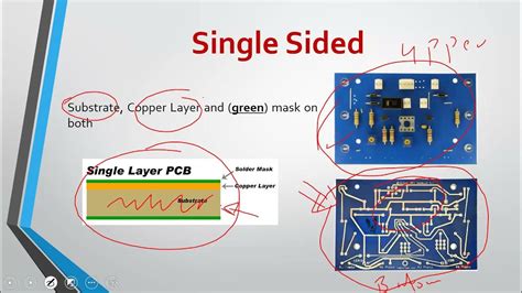
Single Layer PCBs
Single layer PCBs have conductive copper traces printed on only one side of the board. The components are also soldered on the same side. These are the simplest and cheapest type of PCB, suitable for basic circuits. However, they are limited in complexity and density of components.
Double Layer PCBs
Double layer PCBs have conductive traces on both sides of the board. The two layers are connected using vias – small plated holes that allow signals to pass from one side to the other. This allows for more complex circuits and higher component density compared to single layer boards.
Multi-Layer PCBs
For even more complex circuits, multi-layer PCBs are used. These have three or more conductive layers sandwiched between insulating layers. The inner layers are connected using vias. More layers allow for higher component density and more intricate circuit designs. Multi-layer PCBs are used in advanced electronics like smartphones, computers, and medical devices.
| PCB Type | Layers | Complexity | Cost |
|---|---|---|---|
| Single Layer | 1 | Low | $ |
| Double Layer | 2 | Medium | $$ |
| Multi-Layer | 3+ | High | $$$ |
Rigid PCBs
Most PCBs are rigid, meaning they are made from solid, inflexible material like fiberglass. The rigidity provides mechanical support for the components. Rigid PCBs are suitable for most applications where the board does not need to bend or flex.
Flexible PCBs
Flexible PCBs, or flex PCBs, are made from thin, flexible plastic materials like polyimide. The conductive traces are also printed on this flexible substrate. Flex PCBs can bend and twist without breaking, making them ideal for applications where the circuit needs to fit in tight spaces or move with other mechanical parts. Examples include cable connectors, wearable electronics, and foldable smartphones.
Rigid-Flex PCBs
Rigid-flex PCBs are a combination of rigid and flexible sections. Some parts of the board are rigid to support components, while other parts are flexible to allow bending. This combines the benefits of both types – mechanical support where needed and flexibility where required. Rigid-flex PCBs are often used in aerospace and military applications.

PCB Design Process
Designing a PCB involves several steps, usually done using specialized software called Electronic Design Automation (EDA) tools.
-
Schematic Capture: The first step is to create a schematic diagram of the circuit. This is a graphical representation showing how the components are connected, but not their physical layout. EDA software is used to draw the schematic and specify component values.
-
Component Placement: Once the schematic is complete, the components need to be placed on the board. This is done in the EDA software’s PCB layout editor. The designer positions the component footprints (the copper pads to which the component pins will be soldered) and defines the board outline.
-
Routing: After component placement, the conductive traces need to be routed to connect the components according to the schematic. This is usually done automatically by the EDA tool, but the designer can manually adjust the routing if needed. The goal is to minimize the length of traces and avoid interference.
-
Design Rule Check (DRC): Before finalizing the design, a DRC is performed. This is an automated check to ensure the PCB layout meets the manufacturing specifications, such as minimum trace width, clearance between traces, and hole sizes. Any violations are flagged for the designer to fix.
-
Gerber File Generation: Once the design is finalized and passes DRC, Gerber files are generated. These are the industry standard files that describe the PCB layout in a format that can be understood by PCB manufacturers. A set of Gerber files includes separate files for each conductive layer, solder mask, silk screen, and drill holes.

PCB Manufacturing Process
After the PCB design is complete and Gerber files are generated, the board is ready for manufacturing. The manufacturing process involves several steps:
- PCB Fabrication: The bare PCB is fabricated based on the Gerber files. This involves the following sub-steps:
a. Printing: The conductive pattern for each layer is printed onto copper-clad laminate sheets using photoresist and etched using chemicals, leaving only the desired copper traces.
b. Lamination: For multi-layer boards, the individual layers are aligned and laminated together under high temperature and pressure.
c. Drilling: Holes are drilled through the board for vias and component leads.
d. Plating: The holes are plated with copper to create electrical connections between layers.
e. Solder Mask Application: A protective solder mask is applied over the copper traces, leaving only the pads exposed.
f. Silkscreen: Text and symbols are printed onto the board for component identification and assembly instructions.
- PCB Assembly (PCBA): The fabricated PCB is populated with components. This can be done in two ways:
a. Through-Hole Assembly: For through-hole components, the leads are inserted into holes drilled in the board and soldered in place.
b. Surface Mount Assembly: For surface mount components, the parts are placed directly onto pads on the board’s surface and soldered using reflow ovens.
- Inspection and Testing: After assembly, the completed board goes through visual inspection and electrical testing to ensure proper functionality before being shipped.

PCB Design Considerations
When designing a PCB, there are several key factors to consider to ensure optimal performance and manufacturability:
Signal Integrity
Maintaining signal integrity is crucial, especially in high-speed circuits. This involves minimizing crosstalk between traces, controlling impedance, and proper termination. Techniques like ground planes, proper trace routing, and differential signaling are used to maintain signal integrity.
Power Integrity
Providing clean and stable power to all components is essential. This involves proper power plane design, decoupling capacitors, and minimizing voltage drop across the board. Power distribution network (PDN) analysis is used to optimize the power delivery system.
Electromagnetic Compatibility (EMC)
PCBs can both emit and be susceptible to electromagnetic interference (EMI). Proper EMC design techniques are needed to minimize emissions and increase immunity. This includes proper grounding, shielding, filtering, and layout techniques like keeping high-speed traces away from board edges.
Thermal Management
As components consume power, they generate heat which must be dissipated to prevent overheating and failure. PCB thermal management involves techniques like copper pours, thermal vias, and proper component placement to distribute heat evenly.
Manufacturing Considerations
The PCB design must adhere to the capabilities of the manufacturing process. This includes factors like minimum trace width and spacing, hole sizes, and solder mask clearances. Designers must work closely with the manufacturer and adhere to their design rules to ensure manufacturability.
Frequently Asked Questions
Q: What is the difference between through-hole and surface mount components?
A: Through-hole components have long metal leads that are inserted into holes drilled in the PCB and soldered in place. Surface mount components have small metal pads that are soldered directly onto the surface of the PCB. Surface mount components are smaller and allow for higher component density, but through-hole components are easier to solder manually and provide stronger mechanical connections.
Q: What is the purpose of solder mask on a PCB?
A: Solder mask is a protective layer applied over the copper traces on a PCB, leaving only the pads exposed. It serves several purposes:
- Prevents accidental short circuits by insulating the traces
- Protects the copper from oxidation and contamination
- Provides a better surface for the solder to adhere to during assembly
- Improves the aesthetics of the board by providing a uniform color (usually green)
Q: What are vias in a PCB?
A: Vias are small plated holes that allow signals to pass from one layer of a PCB to another. They are used to route traces between layers in multi-layer boards. There are several types of vias:
- Through vias: go through the entire thickness of the board
- Blind vias: start on an outer layer and end on an inner layer
- Buried vias: start and end on inner layers
- Microvias: very small vias used in high-density designs
Q: What is the role of a ground plane in a PCB?
A: A ground plane is a large area of copper, usually on an inner layer of a multi-layer PCB, that is connected to the circuit’s ground. It serves several important functions:
- Provides a low-impedance return path for currents, which is essential for maintaining signal integrity
- Shields signals on adjacent layers from each other, reducing crosstalk
- Distributes heat evenly across the board, aiding in thermal management
- Acts as a reference plane for controlled impedance traces
Q: What files do I need to provide to a PCB manufacturer?
A: To have a PCB manufactured, you typically need to provide the following files:
- Gerber files: These describe the copper patterns for each layer, solder mask, and silkscreen. A separate file is provided for each layer.
- Drill files: These specify the location, size, and type of all the holes in the board.
- Bill of Materials (BOM): This lists all the components used in the design, along with their quantities and part numbers.
- Assembly drawings: These show where each component is placed on the board and in what orientation.
- Any special instructions or requirements for the manufacturer.
Conclusion
PCBs are the backbone of modern electronics. Understanding the basics of PCB types, design process, manufacturing, and key considerations is essential for anyone involved in electronics design and production.
As PCB technology continues to advance, with increasing miniaturization, higher speeds, and more complex functionality, a solid grasp of these fundamentals becomes even more critical. By mastering the basics, designers can create PCBs that are reliable, high-performing, and manufacturable, paving the way for the next generation of electronic devices.
Leave a Reply