Introduction to PCB Assembly and Panelization
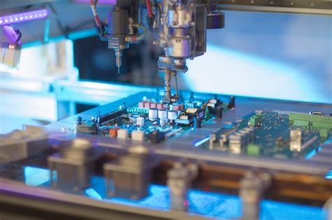
Printed Circuit Board (PCB) assembly is a crucial process in the electronics manufacturing industry. It involves the placement and soldering of electronic components onto a printed circuit board to create a functional electronic device. One of the key aspects of PCB assembly is panelization, which refers to the process of arranging multiple PCBs on a larger panel for efficient production.
Panelization offers several benefits in PCB assembly, including:
- Increased production efficiency
- Reduced manufacturing costs
- Improved handling and transportation
- Consistency in PCB quality
To achieve optimal results in PCB assembly, it is essential to understand and adhere to the panel requirements. This article will delve into the various aspects of panel requirements for PCB assembly, covering topics such as panel size, material selection, tooling holes, fiducial marks, and more.
Standard Panel Sizes for PCB Assembly
When it comes to panel sizes for PCB assembly, there are several standard dimensions to consider. These standard sizes ensure compatibility with various manufacturing equipment and processes. Some of the most common panel sizes include:
| Panel Size | Dimensions (mm) | Dimensions (inches) |
|---|---|---|
| 1/8 Panel | 125 x 250 | 4.92 x 9.84 |
| 1/4 Panel | 250 x 250 | 9.84 x 9.84 |
| 1/2 Panel | 250 x 500 | 9.84 x 19.69 |
| Full Panel | 500 x 500 | 19.69 x 19.69 |
It’s important to note that these dimensions are approximate and may vary slightly depending on the manufacturer and specific requirements of the PCB assembly project.
Choosing the Right Panel Size
When selecting a panel size for your PCB assembly project, consider the following factors:
- PCB dimensions: Ensure that the individual PCB dimensions fit within the chosen panel size, allowing for adequate spacing and tooling holes.
- Production quantity: Higher production quantities may benefit from larger panel sizes to maximize efficiency and reduce costs.
- Manufacturing equipment: Verify that the selected panel size is compatible with the available manufacturing equipment, such as pick-and-place machines and reflow ovens.
- Material availability: Some PCB materials may have limitations on the maximum panel size available.
By carefully evaluating these factors, you can determine the most suitable panel size for your specific PCB assembly project.

Panel Material Selection
The choice of panel material is another critical aspect of panel requirements for PCB assembly. The most commonly used materials for PCB Panels are:
- FR-4: A flame-retardant, glass-reinforced epoxy laminate that offers excellent mechanical and electrical properties. FR-4 is the most widely used material for PCB substrates.
- Aluminum: Used for PCBs that require enhanced thermal dissipation, such as high-power applications or LED lighting.
- Polyimide: A high-temperature, flexible material suitable for applications that demand flexibility or resistance to extreme temperatures.
- CEM-3: A composite epoxy material that combines woven glass fabric and paper reinforcement. CEM-3 is a cost-effective alternative to FR-4 for less demanding applications.
When selecting a panel material, consider the following factors:
- Electrical requirements (dielectric constant, loss tangent, etc.)
- Thermal requirements (heat dissipation, thermal expansion)
- Mechanical requirements (strength, rigidity, flexibility)
- Environmental factors (temperature range, humidity, chemical exposure)
- Cost and availability

Tooling Holes and Fiducial Marks
Tooling holes and fiducial marks are essential features of PCB panels that facilitate accurate positioning and alignment during the assembly process.
Tooling Holes
Tooling holes are precision-drilled holes located on the edges of the panel, used for securing the panel in place during various manufacturing stages. They ensure consistent positioning and prevent shifting or movement of the panel.
Key considerations for tooling holes include:
- Size: Tooling hole sizes typically range from 2.0 mm to 3.2 mm in diameter, depending on the panel size and manufacturing equipment.
- Location: Tooling holes should be positioned at a sufficient distance from the edge of the panel to avoid weakening the panel structure. A minimum distance of 5 mm is generally recommended.
- Quantity: The number of tooling holes required depends on the panel size and the specific manufacturing process. Typically, a minimum of three tooling holes is used for stable positioning.
Fiducial Marks
Fiducial marks are precise reference points on the PCB panel that enable accurate alignment and positioning of components during the assembly process. They are especially critical for surface mount technology (SMT) assembly, where high precision is required.
Fiducial marks should adhere to the following guidelines:
- Shape: Fiducial marks are typically circular, with a diameter ranging from 1.0 mm to 2.0 mm. The shape should be consistent across all fiducial marks on the panel.
- Placement: Fiducial marks should be located near the corners of the panel, close to the individual PCBs. A minimum of three fiducial marks is recommended for accurate alignment.
- Contrast: Fiducial marks should have high contrast against the PCB substrate to ensure reliable detection by machine vision systems. Copper or soldermask-defined fiducials are commonly used.
By incorporating well-designed tooling holes and fiducial marks, you can ensure precise alignment and positioning throughout the PCB assembly process, resulting in higher quality and reliability of the final product.

Panelization Techniques
There are several panelization techniques used in PCB assembly to arrange multiple PCBs on a single panel. The choice of technique depends on factors such as PCB design, production volume, and assembly requirements. Some common panelization techniques include:
- Tab-routed panels: PCBs are connected to the main panel using tabs, which are later broken off after assembly. This technique is suitable for simple PCB designs and low-volume production.
- Scored panels: PCBs are separated by v-shaped grooves cut into the panel, allowing for easy separation after assembly. Scored panels are ideal for medium to high-volume production and offer improved efficiency compared to tab-routed panels.
- Perforated panels: PCBs are connected to the main panel by a series of small, drilled holes along the perimeter of each board. This technique provides a clean break between the PCBs and the panel, reducing stress on the components during separation.
- Frameless panels: PCBs are closely arranged on the panel without any connecting tabs or frames. This technique maximizes panel utilization and is suitable for high-volume production, but requires specialized handling and separation equipment.
When selecting a panelization technique, consider the following factors:
- PCB design complexity
- Component placement and clearances
- Production volume and efficiency
- Assembly equipment capabilities
- Depanelization method and requirements
Spacing and Clearance Requirements
Proper spacing and clearance between PCBs on a panel are crucial for ensuring reliable assembly and preventing damage to components during the depanelization process.
Border Clearance
Border clearance refers to the minimum distance between the edge of the PCB and the edge of the panel. This space accommodates tooling holes, fiducial marks, and any necessary panel identification markings. A minimum border clearance of 5 mm is typically recommended.
Inter-PCB Spacing
Inter-PCB spacing is the distance between adjacent PCBs on the panel. Adequate spacing is necessary to prevent any interference between components on neighboring boards during the assembly process. The minimum inter-PCB spacing depends on several factors, including:
- Component height: Taller components require greater spacing to avoid collisions during placement and soldering.
- Assembly equipment: The capabilities of the assembly equipment, such as the minimum clearance required for pick-and-place nozzles, influence the spacing requirements.
- Panelization technique: Different panelization techniques may have specific spacing requirements to ensure proper separation of the PCBs after assembly.
As a general guideline, a minimum inter-PCB spacing of 2 mm to 3 mm is recommended, but this may vary based on the specific project requirements.
Depanelization Clearance
Depanelization clearance refers to the space required around each PCB to accommodate the depanelization process, which involves separating the individual PCBs from the panel after assembly. The clearance required depends on the depanelization method used, such as:
- V-scoring: A minimum clearance of 1 mm is typically recommended for v-scored panels to ensure clean breakage without damaging the PCBs.
- Tab-routing: Tab-routed panels require sufficient clearance around the tabs to allow for clean removal without stressing the components. A minimum tab width of 2 mm and a clearance of 1 mm around the tabs are common.
- Perforated panels: Perforated panels require adequate spacing between the holes and the PCB Edges to maintain structural integrity during handling and assembly.
By adhering to the recommended spacing and clearance requirements, you can ensure smooth PCB assembly and minimize the risk of damage during the depanelization process.
Panel Identification and Markings
Panel identification and markings are essential for traceability and quality control throughout the PCB assembly process. Clear and consistent labeling helps to track panels, identify issues, and maintain accurate records.
Panel Identification
Each panel should be uniquely identified using a combination of text and barcodes. The following information is typically included in panel identification:
- Panel number: A unique alphanumeric code assigned to each panel for tracking purposes.
- Revision number: Indicates the version of the PCB design or any modifications made to the panel.
- Date code: Specifies the date of panel fabrication, usually in the format YYMMDD.
- Manufacturer identification: Identifies the PCB fabrication facility or company.
Panel identification markings should be placed in a consistent location on the panel, such as the border area, and should be clearly visible and readable.
Barcode Labeling
In addition to text-based identification, panels often include barcodes for automated tracking and data capture. Barcodes streamline the process of panel tracking and reduce the risk of human error. Some common barcode formats used in PCB assembly include:
- Code 128: A high-density, alphanumeric barcode format that supports a wide range of characters and is widely used in the electronics industry.
- Data Matrix: A two-dimensional barcode that can store a large amount of information in a small space, making it ideal for panel identification.
Barcodes should be placed in a consistent location on the panel, preferably near the text-based identification markings, and should be of sufficient size and quality to ensure reliable scanning.
Fiducial Marking
As discussed earlier, fiducial marks are critical for accurate component placement during PCB assembly. In addition to the main fiducial marks used for alignment, panels may include additional fiducial markings for specific purposes, such as:
- Tooling hole fiducials: Used to verify the position and alignment of tooling holes.
- Panel corner fiducials: Placed at the corners of the panel to assist with overall panel alignment.
Fiducial markings should follow the same guidelines as the main fiducial marks, ensuring high contrast and precise positioning.
By implementing clear and consistent panel identification and markings, you can enhance traceability, streamline the assembly process, and improve overall quality control.
Best Practices for Panel Design
Designing panels for PCB assembly requires careful consideration of various factors to ensure optimal manufacturability, efficiency, and quality. Here are some best practices to follow when designing panels for PCB assembly:
- Adhere to standard panel sizes: Whenever possible, design your panels to conform to standard panel sizes to ensure compatibility with common manufacturing equipment and processes.
- Optimize panel utilization: Arrange PCBs on the panel to maximize panel utilization and minimize waste. Consider using panelization software to optimize the layout and spacing of PCBs.
- Maintain consistent orientation: Ensure that all PCBs on the panel have the same orientation to simplify the assembly process and reduce the risk of errors.
- Use appropriate panelization techniques: Select the panelization technique that best suits your PCB design, production volume, and assembly requirements. Consider factors such as component placement, depanelization methods, and assembly equipment capabilities.
- Provide adequate spacing and clearance: Maintain sufficient spacing between PCBs and clearance around components to prevent interference and ensure reliable assembly. Adhere to the recommended border clearance, inter-PCB spacing, and depanelization clearance guidelines.
- Incorporate clear identification and markings: Include unique panel identification, revision numbers, date codes, and manufacturer information on each panel. Use barcodes to facilitate automated tracking and data capture.
- Design for depanelization: Consider the depanelization process when designing panels. Incorporate appropriate breakaway tabs, v-scores, or perforations to ensure clean and safe separation of individual PCBs without damaging components.
- Verify design for manufacturability: Before finalizing your panel design, consult with your PCB assembly provider to ensure that the design is compatible with their manufacturing processes and equipment. Make any necessary adjustments based on their feedback.
By following these best practices, you can create panel designs that are optimized for PCB assembly, leading to improved efficiency, quality, and cost-effectiveness in your manufacturing process.
Conclusion
Understanding and adhering to panel requirements is crucial for successful PCB assembly. By considering factors such as panel size, material selection, tooling holes, fiducial marks, spacing and clearance, identification and markings, and following best practices for panel design, you can ensure optimal manufacturability, efficiency, and quality in your PCB assembly process.
A well-designed panel not only streamlines the assembly process but also contributes to the overall reliability and functionality of the final electronic product. By collaborating closely with your PCB assembly provider and staying updated with industry standards and best practices, you can achieve the best possible results in your PCB assembly projects.
FAQs
-
What is the most common panel size for PCB assembly?
The most common panel size for PCB assembly is the 18″ x 24″ (457 mm x 610 mm) panel, which is compatible with a wide range of manufacturing equipment and processes. -
What is the purpose of tooling holes in PCB panels?
Tooling holes are used to secure the panel in place during various manufacturing stages, ensuring consistent positioning and preventing shifting or movement of the panel. -
What are fiducial marks, and why are they important in PCB assembly?
Fiducial marks are precise reference points on the PCB panel that enable accurate alignment and positioning of components during the assembly process. They are critical for ensuring high precision and reliability, especially in surface mount technology (SMT) assembly. -
How much spacing should be maintained between PCBs on a panel?
The minimum inter-PCB spacing depends on factors such as component height, assembly equipment capabilities, and panelization technique. As a general guideline, a minimum spacing of 2 mm to 3 mm is recommended, but this may vary based on specific project requirements. -
What information should be included in panel identification markings?
Panel identification markings should include a unique panel number, revision number, date code, and manufacturer identification. This information is essential for traceability and quality control throughout the PCB assembly process.
Leave a Reply