What is a PCB Panel?
A PCB panel, also known as a printed circuit board panel or array, is a large board that contains multiple identical printed circuit boards (PCBs) arranged in a matrix. The individual PCBs are connected together with breakaway tabs or mouse bites, allowing them to be easily separated after assembly.
Using PCB panels in the manufacturing process offers several advantages:
- Efficiency: Assembling multiple PCBs simultaneously on a panel increases production throughput and reduces handling time.
- Cost reduction: Panel-based assembly minimizes setup time, material waste, and labor costs compared to assembling individual boards.
- Consistency: Producing PCBs on a panel ensures consistent quality and reduces the risk of damage during handling.
Types of PCB Panels
There are two main types of PCB panels:
-
Multi-Up Panels: These panels contain multiple identical PCBs arranged in a grid pattern. The boards are connected by breakaway tabs or mouse bites, allowing for easy separation after assembly.
-
Stepped Panels: Stepped panels are used when the PCBs have different thicknesses or require different assembly processes. The boards are arranged in steps, with each step having a specific thickness or assembly requirement.
PCB Panel Design Considerations
Designing a PCB panel requires careful consideration of several factors to ensure optimal manufacturability and assembly efficiency. Some key aspects to consider include:
Panel Size and Material
The panel size and material should be selected based on the specific requirements of the PCB design and the manufacturing process. Common panel sizes include:
| Panel Size | Dimensions (mm) |
|---|---|
| Small | 180 x 250 |
| Medium | 250 x 350 |
| Large | 350 x 450 |
The most common panel material is FR-4, a flame-retardant glass-reinforced epoxy laminate. Other materials, such as aluminum or flexible substrates, may be used for specific applications.
Board Orientation and Spacing
The orientation and spacing of the individual PCBs on the panel should be optimized for manufacturing efficiency and to minimize material waste. Consider the following:
- Board Rotation: Rotating the boards by 90 degrees can sometimes lead to better panel utilization and reduced waste.
- Spacing: Adequate spacing between boards is necessary to accommodate breakaway tabs, tooling holes, and any required fiducial marks.
Breakaway Tabs and Mouse Bites
Breakaway tabs and mouse bites are used to connect the individual PCBs on the panel. They should be designed to provide sufficient mechanical strength during assembly while allowing for easy separation afterward.
- Tab Width: Tab width typically ranges from 0.8 mm to 1.5 mm, depending on the board thickness and material.
- Mouse Bites: Mouse bites are small, circular cutouts that perforate the tabs, making it easier to separate the boards. The size and spacing of mouse bites should be carefully designed to maintain panel integrity during assembly.
Fiducial Marks and Tooling Holes
Fiducial marks and tooling holes are essential for accurate positioning and alignment during the assembly process.
- Fiducial Marks: Fiducial marks are small, precise features used by machine vision systems to locate and orient the panel during assembly. A minimum of three fiducial marks should be placed on the panel, preferably near the corners.
- Tooling Holes: Tooling holes are used to secure the panel during manufacturing and assembly. They should be placed in the panel’s corners and along the edges, ensuring compatibility with the manufacturing equipment.
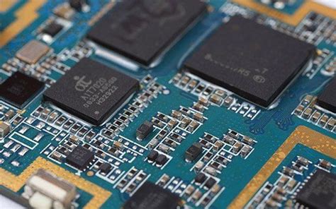
 PCBPanel-a11fb329e77811eebbc9201e88193817.jpeg?resize=1024%2C535&ssl=1″ alt=”” class=”wp-image-136″ srcset=”https://i0.wp.com/rfpcb.org/wp-content/uploads/2024/03/PCBPanel-a11fb329e77811eebbc9201e88193817.jpeg?resize=1024%2C535&ssl=1″ data-recalc-dims=”1″>
Assembly Process Considerations
When designing a PCB panel, it is crucial to consider the specific requirements of the assembly process to ensure compatibility and efficiency.
Solder Paste Application
Solder paste is applied to the PCB pads using a stencil or solder paste printer. The panel design should take into account the following:
- Stencil Thickness: The stencil thickness should be selected based on the component pitch and solder paste requirements. Typical stencil thicknesses range from 0.1 mm to 0.2 mm.
- Aperture Design: The stencil apertures should be designed to ensure optimal solder paste release and to avoid bridging between pads.
Component Placement
The component placement process involves picking and placing components onto the PCB pads. Consider the following when designing the panel:
- Component Clearance: Ensure adequate clearance between components to avoid interference during placement and to facilitate inspection and rework.
- Placement Sequence: Optimize the component placement sequence to minimize the distance traveled by the pick-and-place head, reducing assembly time and improving efficiency.
Reflow Soldering
Reflow soldering is the process of melting the solder paste to form a permanent connection between the components and the PCB pads. The panel design should consider:
- Thermal Mass: Ensure that the panel’s thermal mass is evenly distributed to achieve consistent heating and cooling during reflow.
- Component Compatibility: Verify that all components are compatible with the reflow temperature profile and can withstand the peak temperature without damage.

Design for Manufacturing (DFM) Guidelines
To ensure the best possible manufacturability and assembly efficiency, follow these Design for Manufacturing (DFM) guidelines when creating a PCB panel:
- Minimize Panel Complexity: Keep the panel design as simple as possible, avoiding unnecessary features or complex shapes that may hinder manufacturing or assembly.
- Maintain Consistent Board Thickness: Ensure that all boards on the panel have the same thickness to avoid issues during solder paste application and reflow soldering.
- Use Standard Component Sizes: Whenever possible, use standard component sizes and packages to simplify the assembly process and reduce the risk of errors.
- Provide Adequate Clearances: Maintain sufficient clearances between components, tracks, and board edges to minimize the risk of short circuits and to facilitate inspection and rework.
- Follow Manufacturer Guidelines: Consult with your PCB manufacturer and assembly provider to ensure that your panel design complies with their specific guidelines and requirements.

Frequently Asked Questions (FAQ)
1. What is the optimal panel size for my PCB design?
The optimal panel size depends on your specific PCB design and the manufacturing process. Consult with your PCB manufacturer to determine the most suitable panel size for your project, taking into account factors such as board dimensions, quantity, and assembly requirements.
2. How do I determine the appropriate spacing between boards on a panel?
The spacing between boards on a panel should be determined based on several factors, including the board size, panel material, and assembly process requirements. As a general rule, a minimum spacing of 3-5 mm between boards is recommended to accommodate breakaway tabs, tooling holes, and fiducial marks. However, it’s best to consult with your PCB manufacturer for specific guidance.
3. What are the advantages of using a stepped panel for PCB Assembly?
Stepped panels are advantageous when assembling PCBs with different thicknesses or those requiring different assembly processes. By arranging the boards in steps, each with a specific thickness or assembly requirement, the manufacturing process can be optimized for each board type, improving efficiency and reducing the risk of errors.
4. How can I ensure my PCB panel design is compatible with the assembly process?
To ensure compatibility with the assembly process, consider the following:
- Consult with your PCB assembly provider to understand their specific requirements and guidelines.
- Design your panel with the assembly process in mind, taking into account factors such as solder paste application, component placement, and reflow soldering.
- Follow DFM guidelines to minimize panel complexity, maintain consistent board thickness, use standard component sizes, provide adequate clearances, and adhere to manufacturer guidelines.
5. What are the most common issues encountered when designing PCB panels, and how can I avoid them?
Some common issues encountered when designing PCB panels include:
- Inadequate spacing: Insufficient spacing between boards can lead to manufacturing and assembly difficulties. Ensure adequate spacing to accommodate breakaway tabs, tooling holes, and fiducial marks.
- Inconsistent board thickness: Varying board thicknesses within a panel can cause issues during solder paste application and reflow soldering. Maintain consistent board thickness throughout the panel.
- Incompatible component sizes: Using non-standard or incompatible component sizes can complicate the assembly process. Whenever possible, use standard component sizes and packages.
- Insufficient clearances: Inadequate clearances between components, tracks, and board edges can result in short circuits and hinder inspection and rework. Provide sufficient clearances based on manufacturer guidelines.
To avoid these issues, follow DFM guidelines, consult with your PCB manufacturer and assembly provider, and carefully consider the specific requirements of your PCB design and the manufacturing process.
Conclusion
Designing a PCB panel for efficient assembly requires careful consideration of various factors, including panel size and material, board orientation and spacing, breakaway tabs and mouse bites, fiducial marks and tooling holes, and the specific requirements of the assembly process. By following DFM guidelines and working closely with your PCB manufacturer and assembly provider, you can create a panel design that optimizes manufacturability, reduces costs, and ensures consistent quality.
When designing your PCB panel, remember to:
- Select the appropriate panel size and material based on your PCB design and manufacturing requirements.
- Optimize board orientation and spacing to maximize panel utilization and minimize waste.
- Design breakaway tabs and mouse bites to provide mechanical strength during assembly while allowing for easy separation.
- Include fiducial marks and tooling holes for accurate positioning and alignment during the assembly process.
- Consider the specific requirements of solder paste application, component placement, and reflow soldering.
- Follow DFM guidelines to minimize panel complexity, maintain consistent board thickness, use standard component sizes, provide adequate clearances, and adhere to manufacturer guidelines.
By adhering to these guidelines and best practices, you can streamline the PCB assembly process, reduce costs, and ensure the highest quality for your PCB projects.
Leave a Reply