Introduction to PCB Assembly
Printed Circuit Board (PCB) assembly is a crucial process in the manufacturing of electronic devices. It involves the placement and soldering of electronic components onto a printed circuit board to create a functional electronic circuit. PCB assembly is a complex process that requires precision, accuracy, and attention to detail to ensure the quality and reliability of the final product.
RAYPCB is a leading provider of PCB assembly services, offering a range of solutions for customers across various industries. With state-of-the-art facilities and a team of experienced professionals, RAYPCB is committed to delivering high-quality PCB assembly services that meet the unique needs of each customer.
The Importance of PCB Assembly
PCB assembly plays a critical role in the functionality and performance of electronic devices. A well-designed and properly assembled PCB ensures that the electronic components are connected correctly and securely, which is essential for the device to operate as intended. Poor PCB assembly can lead to a range of issues, including:
- Shorts and open circuits
- Incorrect component placement
- Weak or incomplete solder joints
- Damaged components
- Reduced reliability and durability
By investing in high-quality PCB assembly services, manufacturers can ensure that their electronic devices are reliable, durable, and perform as expected.
The PCB Assembly Process at RAYPCB
The PCB assembly process at RAYPCB involves several key steps, each of which is carefully controlled and monitored to ensure the highest level of quality and reliability.
Step 1: Design and Prototyping
The first step in the PCB assembly process is the design and prototyping phase. During this phase, the customer provides RAYPCB with the design files for their PCB, including the schematic, bill of materials (BOM), and Gerber files. RAYPCB’s team of experienced engineers reviews the design files to ensure that they are complete, accurate, and meet the customer’s specifications.
If necessary, RAYPCB can also provide design assistance to help customers optimize their PCB design for manufacturability and reliability. This may involve making recommendations for component selection, layout, and routing to ensure that the PCB can be assembled efficiently and effectively.
Once the design is finalized, RAYPCB can produce prototypes of the PCB for testing and validation. Prototyping allows customers to verify that the PCB design meets their requirements and to make any necessary adjustments before moving into full-scale production.
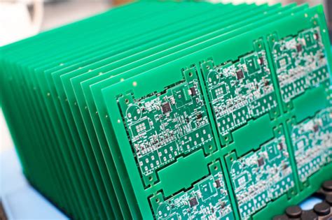
Step 2: PCB Fabrication
The next step in the PCB assembly process is the fabrication of the bare PCB. This involves the following sub-steps:
-
Printing: The PCB design is printed onto a copper-clad laminate material using a high-resolution printer.
-
Etching: The unwanted copper is removed from the laminate using a chemical etching process, leaving only the desired circuit pattern.
-
Drilling: Holes are drilled into the PCB to accommodate through-hole components and vias.
-
Plating: The holes are plated with copper to create electrical connections between the layers of the PCB.
-
Solder Mask Application: A solder mask is applied to the PCB to protect the copper traces from oxidation and to prevent solder bridging during the assembly process.
-
Silkscreen Printing: Text and symbols are printed onto the PCB using a silkscreen process to aid in the assembly process and to provide information about the PCB.
Step 3: Component Placement
Once the bare PCB has been fabricated, the next step is to place the electronic components onto the board. This is typically done using one of two methods: through-hole or surface mount.
Through-Hole Component Placement
Through-hole components have leads that are inserted into holes drilled in the PCB and soldered to pads on the opposite side of the board. Through-hole component placement is typically done manually or using a semi-automatic machine.
Surface Mount Component Placement
Surface mount components are placed directly onto pads on the surface of the PCB and soldered in place. Surface mount component placement is typically done using a pick-and-place machine, which uses a vacuum nozzle to pick up the components from a reel or tray and place them onto the PCB with high precision.
Step 4: Soldering
After the components have been placed onto the PCB, they must be soldered in place to create electrical connections. There are two main methods of soldering: wave soldering and reflow soldering.
Wave Soldering
Wave soldering is used for through-hole components. The PCB is passed over a wave of molten solder, which flows into the holes and creates a solder joint between the component leads and the PCB pads.
Reflow Soldering
Reflow soldering is used for surface mount components. The PCB is heated in a reflow oven, which melts the solder paste applied to the pads during the component placement process. The molten solder then flows around the component leads and creates a solder joint as it cools.
Step 5: Inspection and Testing
After the soldering process is complete, the PCB undergoes a series of inspections and tests to ensure that it meets the required quality standards. This may include:
- Visual inspection to check for defects such as solder bridges, poor solder joints, or missing components
- Automated optical inspection (AOI) to check for component placement accuracy and solder joint quality
- X-ray inspection to check for hidden defects such as voids or cracks in solder joints
- Functional testing to verify that the PCB operates as intended
- In-circuit testing (ICT) to test the electrical connectivity and functionality of individual components on the PCB
Any defects or issues identified during the inspection and testing process are addressed before the PCB is considered complete.
Step 6: Final Assembly and Packaging
Once the PCB has passed all inspections and tests, it is ready for final assembly and packaging. This may involve:
- Installing the PCB into a housing or enclosure
- Attaching cables, connectors, or other components
- Applying labels or markings for identification and tracking purposes
- Packaging the PCB for shipping and delivery to the customer

Benefits of Working with RAYPCB for PCB Assembly
Working with RAYPCB for PCB assembly offers several key benefits for customers:
1. Expertise and Experience
RAYPCB has a team of experienced professionals with deep expertise in PCB design, fabrication, and assembly. This expertise ensures that customers receive high-quality PCBs that meet their specific requirements and are optimized for manufacturability and reliability.
2. State-of-the-Art Facilities
RAYPCB’s PCB assembly facilities are equipped with the latest technology and equipment, including high-speed pick-and-place machines, reflow ovens, and automated inspection systems. This ensures that PCBs are assembled efficiently and to the highest quality standards.
3. Flexibility and Customization
RAYPCB offers a range of PCB assembly services that can be customized to meet the unique needs of each customer. Whether a customer needs a small batch of prototype PCBs or a large production run, RAYPCB can provide a solution that fits their requirements.
4. Quality Control
RAYPCB has a rigorous quality control process in place to ensure that every PCB meets the required quality standards. This includes multiple inspections and tests throughout the assembly process, as well as a final functional test to verify that the PCB operates as intended.
5. Fast Turnaround Times
RAYPCB understands the importance of time-to-market for its customers. That’s why the company offers fast turnaround times for PCB assembly, with standard lead times of 7-10 days for prototype orders and 2-3 weeks for production orders.
6. Competitive Pricing
RAYPCB offers competitive pricing for its PCB assembly services, without compromising on quality or reliability. The company works closely with customers to understand their budget constraints and to provide a solution that meets their needs while staying within their budget.

Conclusion
PCB assembly is a critical process in the manufacturing of electronic devices, and working with a reliable and experienced PCB assembly provider is essential for ensuring the quality and reliability of the final product. RAYPCB is a leading provider of PCB assembly services, offering a range of solutions for customers across various industries.
With state-of-the-art facilities, a team of experienced professionals, and a commitment to quality and customer satisfaction, RAYPCB is well-positioned to meet the PCB assembly needs of customers in today’s fast-paced and constantly evolving electronic industry.

FAQs
1. What is PCB assembly?
PCB assembly is the process of placing and soldering electronic components onto a printed circuit board (PCB) to create a functional electronic circuit.
2. What are the different methods of PCB assembly?
The two main methods of PCB assembly are through-hole assembly and surface mount assembly. Through-hole assembly involves inserting component leads into holes drilled in the PCB and soldering them in place, while surface mount assembly involves placing components directly onto pads on the surface of the PCB and soldering them in place.
3. What are the benefits of working with RAYPCB for PCB assembly?
Working with RAYPCB for PCB assembly offers several key benefits, including expertise and experience, state-of-the-art facilities, flexibility and customization, rigorous quality control, fast turnaround times, and competitive pricing.
4. How long does PCB assembly take at RAYPCB?
RAYPCB offers fast turnaround times for PCB assembly, with standard lead times of 7-10 days for prototype orders and 2-3 weeks for production orders.
5. What industries does RAYPCB serve for PCB assembly?
RAYPCB serves customers across a range of industries, including automotive, medical, aerospace, consumer electronics, and industrial automation, among others. The company’s PCB assembly services are tailored to meet the unique needs and requirements of each industry.
Leave a Reply