What is a PCB?
A printed circuit board (PCB) is a flat board made of insulating material, such as fiberglass or plastic, with conductive copper traces etched onto its surface. These traces connect various electronic components, like resistors, capacitors, and integrated circuits, to form a complete electronic circuit. PCBs are used in almost all electronic devices, from simple consumer gadgets to complex industrial equipment.
Types of PCBs
There are several types of PCBs, each with its own unique characteristics and applications:
-
Single-layer PCB: A single-layer PCB has conductive traces on only one side of the board. These are the simplest and most cost-effective PCBs, suitable for basic electronic projects.
-
Double-layer PCB: A double-layer PCB has conductive traces on both sides of the board, allowing for more complex circuits and higher component density. The two layers are connected through vias (small holes) drilled through the board.
-
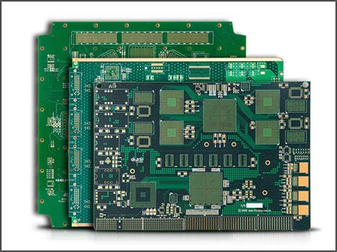
Multi-layer PCB: A multi-layer PCB consists of three or more layers of conductive traces, separated by insulating layers. These PCBs offer the highest component density and are used in complex electronic devices, such as smartphones and computers.
-
Flexible PCB: A flexible PCB is made of a thin, flexible insulating material, allowing the board to bend and fold. These PCBs are used in applications where space is limited or where the board needs to conform to a specific shape.
-
Rigid-Flex PCB: A rigid-flex PCB combines the features of rigid and flexible PCBs, with rigid sections for mounting components and flexible sections for connecting them. This type of PCB is used in applications that require both stability and flexibility.
PCB Manufacturing Process
The PCB manufacturing process involves several steps, each of which is critical to ensuring the quality and reliability of the final product.
Step 1: Design
The first step in PCB manufacturing is designing the circuit and creating the PCB layout using specialized software, such as Altium Designer or Eagle. The design includes the placement of components, the routing of conductive traces, and the creation of solder masks and silkscreens.
Step 2: Printing
Once the design is complete, the PCB layout is printed onto a transparent film or directly onto the copper-clad board using a photoplotter or laser printer. This process creates a photomask, which will be used in the next step.
Step 3: Etching
The copper-clad board is coated with a light-sensitive resist and then exposed to UV light through the photomask. The exposed areas of the resist harden, while the unexposed areas remain soluble. The board is then developed, removing the soluble resist and exposing the copper underneath. Finally, the board is placed in an etching solution, which removes the exposed copper, leaving only the desired conductive traces.
Step 4: Drilling
After etching, holes are drilled through the board to accommodate through-hole components and vias. The drilling process is typically done using a computer-controlled drill machine.
Step 5: Solder Mask Application
A solder mask, usually green in color, is applied to the board to protect the copper traces from oxidation and to prevent solder bridges from forming between closely spaced traces. The solder mask also provides insulation and improves the board’s appearance.
Step 6: Silkscreen Printing
A silkscreen layer is printed onto the board to add text, logos, and component identifiers. This layer helps in the assembly process and makes it easier to identify components and their orientations.
Step 7: Surface Finish
A surface finish, such as HASL (Hot Air Solder Leveling), ENIG (Electroless Nickel Immersion Gold), or OSP (Organic Solderability Preservative), is applied to the exposed copper pads to prevent oxidation and improve solderability.
Step 8: Electrical Testing
After the manufacturing process is complete, the PCB undergoes electrical testing to ensure that all connections are correct and that there are no short circuits or open connections.
| Step | Process | Description |
|---|---|---|
| 1 | Design | Create PCB layout using specialized software |
| 2 | Printing | Print PCB layout onto photomask |
| 3 | Etching | Remove unwanted copper to create conductive traces |
| 4 | Drilling | Drill holes for through-hole components and vias |
| 5 | Solder Mask Application | Apply solder mask to protect traces and provide insulation |
| 6 | Silkscreen Printing | Print text, logos, and component identifiers |
| 7 | Surface Finish | Apply surface finish to prevent oxidation and improve solderability |
| 8 | Electrical Testing | Test PCB for correct connections and potential issues |

PCB Design Considerations
When designing a PCB, there are several key factors to consider to ensure optimal performance, reliability, and manufacturability.
Component Placement
Proper component placement is crucial for several reasons:
-
Signal integrity: Components should be placed in a way that minimizes the length of critical signal paths, reduces crosstalk, and avoids electromagnetic interference (EMI).
-
Thermal management: Heat-generating components, such as power regulators and processors, should be placed in a way that allows for efficient heat dissipation.
-
Mechanical constraints: Component placement must account for mechanical constraints, such as connector locations and mounting holes.
Trace Routing
Trace routing is the process of creating the conductive paths that connect components on the PCB. When routing traces, consider the following:
-
Trace width: The width of a trace determines its current-carrying capacity and impedance. Wider traces can carry more current and have lower impedance, but they also take up more space on the board.
-
Trace spacing: The spacing between traces affects the board’s manufacturability and signal integrity. Closely spaced traces are more difficult to manufacture and are more susceptible to crosstalk.
-
Via placement: Vias should be placed in a way that minimizes the length of signal paths and reduces the number of layers required.
Power and Ground Planes
Power and ground planes are large copper areas that provide a low-impedance path for power and ground connections. These planes help to reduce EMI, improve signal integrity, and distribute heat more evenly across the board.
Signal Integrity
Signal integrity refers to the quality of the electrical signals transmitted through the PCB. To maintain good signal integrity, consider the following:
-
Impedance matching: Ensure that the impedance of the traces matches the impedance of the source and load to minimize reflections and signal distortion.
-
Termination: Use appropriate termination techniques, such as series termination or parallel termination, to reduce reflections and improve signal quality.
-
Crosstalk reduction: Minimize crosstalk by keeping sensitive traces away from each other, using guard traces, and employing differential signaling when possible.
Manufacturability
To ensure that a PCB can be manufactured reliably and cost-effectively, consider the following:
-
Design for manufacturing (DFM): Follow the manufacturer’s design guidelines for minimum trace width, spacing, and hole size to avoid manufacturing issues.
-
Panelization: Group multiple PCBs into a single panel to reduce manufacturing costs and improve efficiency.
-
Testability: Include test points and other features that facilitate automated testing and inspection.

PCB Assembly
Once a PCB has been manufactured, the next step is to assemble the components onto the board. There are two main methods of PCB assembly: through-hole and surface mount.
Through-Hole Assembly
In through-hole assembly, components with long leads are inserted into holes drilled through the PCB and soldered onto the opposite side. This method is well-suited for larger components and for applications where mechanical strength is important.
Surface Mount Assembly
Surface mount assembly involves placing components directly onto the surface of the PCB and soldering them in place. Surface mount components are smaller and have shorter leads than through-hole components, allowing for higher component density and improved high-frequency performance.
Assembly Process
The PCB assembly process typically involves the following steps:
-
Solder paste application: Solder paste, a mixture of tiny solder particles and flux, is applied to the PCB’s pads using a stencil or syringe.
-
Component placement: Components are placed onto the PCB, either manually or using automated pick-and-place machines.
-
Reflow soldering: The PCB is heated in a reflow oven, melting the solder paste and creating a permanent connection between the components and the board.
-
Inspection: The assembled PCB is inspected for defects, such as solder bridges, cold solder joints, and misaligned components.
-
Rework: Any defects found during inspection are corrected through manual rework or by using specialized rework equipment.

PCB Testing
After assembly, PCBs must undergo various tests to ensure proper functionality and reliability. Some common PCB testing methods include:
In-Circuit Testing (ICT)
ICT involves using a bed-of-nails fixture to make contact with specific points on the PCB and measure the electrical properties of individual components and circuits. This method is useful for detecting component failures, shorts, and opens.
Flying Probe Testing
Flying probe testing uses movable probes to make contact with test points on the PCB. This method is more flexible than ICT but slower and better suited for prototypes and low-volume production.
Functional Testing
Functional testing involves powering up the PCB and verifying that it performs its intended function. This may include running software tests, measuring output signals, and checking for proper communication between components.
Boundary Scan Testing
Boundary scan testing, also known as JTAG testing, uses a special test access port (TAP) built into certain integrated circuits to test the interconnections between components. This method is useful for detecting manufacturing defects and for programming flash memories and FPGAs.
Environmental Testing
Environmental testing exposes the PCB to various environmental conditions, such as temperature extremes, humidity, and vibration, to ensure that it can operate reliably in its intended environment.
Frequently Asked Questions (FAQ)
-
What is the difference between a schematic and a PCB layout?
A schematic is a symbolic representation of an electronic circuit, showing the components and their interconnections. A PCB layout, on the other hand, is a physical representation of the circuit, showing the actual placement of components and the routing of traces on the board. -
What is the purpose of a solder mask on a PCB?
A solder mask is a protective layer applied to the PCB that covers the copper traces, leaving only the pads exposed. The solder mask prevents solder bridges from forming between closely spaced traces, provides electrical insulation, and protects the traces from oxidation and damage. -
What is the difference between through-hole and surface mount components?
Through-hole components have long leads that are inserted into holes drilled through the PCB and soldered onto the opposite side. Surface mount components, on the other hand, are placed directly onto the surface of the PCB and soldered in place. Surface mount components are smaller and have shorter leads, allowing for higher component density and improved high-frequency performance. -
What is the purpose of a power plane on a PCB?
A power plane is a large copper area on a PCB that provides a low-impedance path for power distribution. Power planes help to reduce electromagnetic interference (EMI), improve signal integrity, and distribute heat more evenly across the board. -
What is the difference between a rigid PCB and a flexible PCB?
A rigid PCB is made from a solid, non-flexible material, such as fiberglass or epoxy laminate. A flexible PCB, on the other hand, is made from a thin, flexible material, such as polyimide or polyester. Flexible PCBs are used in applications where the board needs to conform to a specific shape or where space is limited.
Conclusion
PCBs are essential components in modern electronics, providing a reliable and efficient means of interconnecting electronic components. Understanding the basics of PCB design, manufacturing, assembly, and testing is crucial for anyone involved in the development or production of electronic devices.
By considering factors such as component placement, trace routing, signal integrity, and manufacturability, designers can create PCBs that are reliable, cost-effective, and well-suited to their intended applications. As technology continues to advance, the importance of well-designed and well-manufactured PCBs will only continue to grow.
Leave a Reply