Introduction to PCB Testing
Printed Circuit Board (PCB) testing is a crucial step in the manufacturing process of electronic devices. It ensures that the PCB functions as intended and meets the required specifications. PCB testing involves various methods and techniques to verify the quality, reliability, and functionality of the board. In this article, we will discuss the essential aspects of PCB testing that you need to know.
Why is PCB Testing Important?
PCB testing is important for several reasons:
-
Quality Assurance: PCB testing helps to identify defects and issues in the board before it is assembled into the final product. This ensures that only high-quality boards are used, reducing the risk of product failures and recalls.
-
Reliability: Thorough PCB testing ensures that the board can withstand various environmental conditions and operate reliably over its expected lifetime.
-
Cost Savings: Detecting and fixing issues during the testing phase is much more cost-effective than dealing with product failures or returns after the product has been released to the market.
-
Compliance: PCB testing helps to ensure that the board complies with various industry standards and regulations, such as IPC (Institute of Printed Circuits) and UL (Underwriters Laboratories).

Types of PCB Testing
There are various types of PCB testing, each focusing on different aspects of the board’s functionality and quality. Some of the common types of PCB testing include:
Visual Inspection
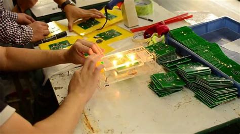
Visual inspection is the first step in PCB testing. It involves examining the board for any visible defects, such as scratches, cracks, or missing components. This can be done manually by trained operators or using automated optical inspection (AOI) systems.
Automated Optical Inspection (AOI)
AOI uses high-resolution cameras and image processing software to automatically inspect the PCB for defects. It can detect issues such as incorrect component placement, solder bridging, and missing or damaged components.
X-Ray Inspection
X-ray inspection is used to examine the internal structure of the PCB, particularly for multi-layer boards. It can detect issues such as voids in solder joints, incorrect layer alignment, and damaged or missing vias.
In-Circuit Testing (ICT)
ICT involves using a bed-of-nails fixture to make electrical contact with specific points on the PCB. This allows for testing individual components and circuits on the board to ensure they function correctly and have the right values.
Flying Probe Testing
Flying probe testing uses movable probes to make electrical contact with various points on the PCB. This method is more flexible than ICT and can be used for low-volume production or prototypes.
Functional Testing
Functional testing involves testing the PCB under real-world operating conditions to ensure that it performs as intended. This can include testing the board’s response to various inputs, measuring output signals, and verifying communication protocols.
Boundary Scan Testing
Boundary scan testing, also known as JTAG (Joint Test Action Group) testing, is a method for testing the interconnections between integrated circuits (ICs) on the PCB. It uses a special test access port (TAP) to control and monitor the ICs’ input and output pins.
Burn-In Testing
Burn-in testing involves subjecting the PCB to elevated temperatures and operating conditions for an extended period to identify any early failures or weaknesses in the board.

PCB Testing Equipment
To perform various types of PCB testing, specialized equipment is required. Some of the common PCB testing equipment includes:
-
Multimeters: Used for measuring voltage, current, and resistance on the PCB.
-
Oscilloscopes: Used for visualizing and measuring time-varying signals on the board.
-
Logic Analyzers: Used for capturing and analyzing digital signals on the PCB.
-
Spectrum Analyzers: Used for measuring the frequency response and signal integrity of the board.
-
Thermal Cameras: Used for detecting hot spots and thermal issues on the PCB.
-
Environmental Chambers: Used for subjecting the PCB to various environmental conditions, such as temperature, humidity, and vibration, to test its reliability and durability.

PCB Testing Standards
To ensure consistency and reliability in PCB testing, various industry standards have been established. Some of the key PCB testing standards include:
- IPC-A-610: Acceptability of Electronic Assemblies
- IPC-6012: Qualification and Performance Specification for Rigid Printed Boards
- IPC-J-STD-001: Requirements for Soldered Electrical and Electronic Assemblies
- IPC-TM-650: Test Methods Manual
- MIL-STD-883: Test Method Standard for Microcircuits
These standards provide guidelines for visual inspection, electrical testing, environmental testing, and other aspects of PCB testing.
Best Practices for PCB Testing
To ensure effective and efficient PCB testing, consider the following best practices:
-
Develop a comprehensive test plan: Define the scope, objectives, and requirements of PCB testing early in the design process.
-
Use appropriate testing methods: Select the right testing methods based on the complexity, volume, and criticality of the PCB.
-
Establish clear acceptance criteria: Define the acceptable limits for various parameters, such as electrical characteristics, visual defects, and functional performance.
-
Maintain proper documentation: Keep accurate records of test results, procedures, and any issues encountered during testing.
-
Continuously improve the testing process: Regularly review and update the testing process based on feedback, new technologies, and changing requirements.
Common PCB Testing Challenges and Solutions
PCB testing can present various challenges, such as:
-
High-density boards: Testing high-density boards with small components and tight spacing can be difficult. Solutions include using advanced testing equipment, such as flying probe testers and X-ray inspection systems.
-
RF and high-speed circuits: Testing high-frequency and high-speed circuits requires specialized equipment and techniques. Solutions include using vector network analyzers, time-domain reflectometers, and signal integrity analysis tools.
-
Flexible and rigid-flex boards: Testing flexible and rigid-flex boards can be challenging due to their unique mechanical properties. Solutions include using specialized fixtures and testing methods, such as bending and twisting tests.
-
Environmental factors: Testing PCBs under various environmental conditions, such as temperature, humidity, and vibration, can be complex. Solutions include using environmental chambers and following standard test methods, such as MIL-STD-810.
Conclusion
PCB testing is a critical aspect of the electronics manufacturing process. It ensures that the PCB functions as intended, meets the required specifications, and can withstand real-world operating conditions. By understanding the various types of PCB testing, equipment, standards, and best practices, you can effectively implement a comprehensive testing strategy for your PCB projects.
Frequently Asked Questions (FAQ)
-
What is the difference between in-circuit testing (ICT) and functional testing?
In-circuit testing focuses on testing individual components and circuits on the PCB, while functional testing evaluates the overall performance of the board under real-world operating conditions. -
How often should PCB testing be performed?
PCB testing should be performed at various stages of the manufacturing process, including prototyping, production, and final assembly. The frequency of testing depends on the complexity, volume, and criticality of the PCB. -
Can PCB testing be automated?
Yes, many aspects of PCB testing can be automated using specialized equipment, such as automated optical inspection (AOI) systems, flying probe testers, and in-circuit testers. -
What are the benefits of using X-ray inspection for PCB testing?
X-ray inspection allows for examining the internal structure of the PCB, particularly for multi-layer boards. It can detect issues such as voids in solder joints, incorrect layer alignment, and damaged or missing vias, which may not be visible through other testing methods. -
How can I ensure that my PCB complies with industry standards?
To ensure compliance with industry standards, refer to the relevant specifications, such as IPC and MIL standards, and follow their guidelines for PCB design, manufacturing, and testing. Additionally, consider working with certified PCB manufacturers and testing services that adhere to these standards.
| PCB Testing Method | Purpose | Advantages | Disadvantages |
|---|---|---|---|
| Visual Inspection | Examine the board for visible defects | Quick and cost-effective | Limited to surface defects, subject to human error |
| Automated Optical Inspection (AOI) | Automatically inspect the PCB for defects using cameras and software | Fast, accurate, and consistent | Cannot detect internal defects, high initial investment |
| X-Ray Inspection | Examine the internal structure of the PCB, particularly multi-layer boards | Can detect internal defects and layer alignment issues | Expensive equipment, requires skilled operators |
| In-Circuit Testing (ICT) | Test individual components and circuits using a bed-of-nails fixture | Can identify specific component failures and circuit issues | Requires custom fixtures, limited to accessible points |
| Flying Probe Testing | Test various points on the PCB using movable probes | Flexible, suitable for low-volume production or prototypes | Slower than ICT, limited to accessible points |
| Functional Testing | Test the PCB under real-world operating conditions | Ensures the board performs as intended in the final application | May not detect all defects, requires specialized setup |
| Boundary Scan Testing | Test interconnections between ICs using a test access port (TAP) | Can test complex boards with limited physical access | Requires ICs with built-in boundary scan support |
| Burn-In Testing | Subject the PCB to elevated temperatures and operating conditions | Identifies early failures and weaknesses in the board | Time-consuming, may not detect all potential issues |
In conclusion, PCB testing is a multifaceted process that involves various methods, equipment, and standards. By implementing a comprehensive testing strategy and following best practices, you can ensure the quality, reliability, and functionality of your PCB projects. Whether you are a designer, manufacturer, or end-user, understanding the importance and intricacies of PCB testing is essential for success in the electronics industry.
Leave a Reply