What is a PCB Stackup?
A PCB stackup refers to the arrangement of copper layers and insulating materials that make up a printed circuit board. It defines the number of layers, their order, and the thickness of each layer. The stackup plays a crucial role in determining the electrical properties, mechanical stability, and manufacturability of a PCB.
Types of PCB Stackups
There are three main types of PCB stackups:
- Single-sided PCB: This is the simplest type of PCB, with components and copper traces on only one side of the board.
- Double-sided PCB: Also known as a two-layer PCB, this type has components and copper traces on both sides of the board.
- Multi-layer PCB: This type of PCB consists of three or more layers of copper, separated by insulating materials. Multi-layer PCBs are used for more complex designs and offer better signal integrity and EMI performance.
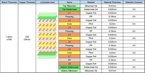
RAYPCB’s Updated Standard Stackup for Multi-layer PCBs
RAYPCB has updated its standard stackup for multi-layer PCBs to optimize signal integrity, power delivery, and manufacturability. The updated stackup incorporates the following features:
- Symmetrical structure for improved mechanical stability and warpage control
- Optimized dielectric materials for better impedance control and signal integrity
- Increased copper weight for power and ground planes to reduce voltage drop and improve current carrying capacity
- Tighter tolerances for layer thickness and alignment to ensure consistent performance
Symmetrical Structure
RAYPCB’s updated stackup employs a symmetrical structure, which means that the layers are arranged in a mirror-like fashion around the center of the board. This symmetry helps to balance the mechanical stresses within the PCB, reducing the risk of warpage and improving overall reliability.
For example, a typical 8-layer PCB stackup with a symmetrical structure would look like this:
| Layer | Material | Thickness (mm) |
|---|---|---|
| 1 | Copper | 0.035 |
| 2 | Prepreg | 0.180 |
| 3 | Copper | 0.035 |
| 4 | Core | 0.400 |
| 5 | Copper | 0.035 |
| 6 | Prepreg | 0.180 |
| 7 | Copper | 0.035 |
| 8 | Solder Mask | 0.025 |
Optimized Dielectric Materials
The updated stackup uses optimized dielectric materials, such as low-loss and high-speed laminates, to improve signal integrity and reduce signal distortion. These materials have better electrical properties, including lower dielectric constant (Dk) and dissipation factor (Df), which help to maintain signal quality and minimize losses.
Some of the commonly used dielectric materials in RAYPCB’s updated stackup include:
- FR-4: A standard PCB material with good mechanical and electrical properties
- IS400: A high-performance material with low Dk and Df, suitable for high-speed applications
- Rogers 4000 series: A family of high-frequency laminates with excellent thermal and electrical properties
Increased Copper Weight for Power and Ground Planes
RAYPCB’s updated stackup features increased copper weight for power and ground planes, typically ranging from 1 oz to 2 oz. This increase in copper thickness helps to reduce voltage drop, improve current carrying capacity, and minimize power supply noise. Thicker copper planes also contribute to better thermal management by dissipating heat more efficiently.
Tighter Tolerances
To ensure consistent performance and manufacturability, RAYPCB has implemented tighter tolerances for layer thickness and alignment in its updated stackup. These stricter tolerances help to maintain the desired impedance values, reduce signal integrity issues, and improve the overall reliability of the PCB.
Some of the key tolerances in RAYPCB’s updated stackup include:
- Layer thickness tolerance: ±10%
- Layer alignment tolerance: ±0.075 mm
- Drilled hole size tolerance: ±0.05 mm

Benefits of RAYPCB’s Updated Standard Stackup
RAYPCB’s updated standard stackup for multi-layer PCBs offers several benefits to customers:
- Improved signal integrity: The optimized dielectric materials and symmetrical structure help to maintain signal quality and reduce distortion, ensuring reliable performance in high-speed applications.
- Better power delivery: The increased copper weight for power and ground planes reduces voltage drop and improves current carrying capacity, resulting in a more stable power supply for the PCB.
- Enhanced mechanical stability: The symmetrical structure and tighter tolerances contribute to better mechanical stability, reducing the risk of warpage and improving the overall reliability of the PCB.
- Faster time-to-market: By using a standard stackup, customers can save time on design and manufacturing, as the stackup has been pre-optimized for performance and manufacturability.
- Cost-effective solution: RAYPCB’s updated standard stackup offers a cost-effective solution for customers, as it eliminates the need for custom stackup development and reduces the risk of design errors and manufacturing issues.

Applications of RAYPCB’s Updated Standard Stackup
RAYPCB’s updated standard stackup for multi-layer PCBs is suitable for a wide range of applications, including:
- Consumer electronics: Smartphones, tablets, laptops, and wearable devices
- Automotive electronics: In-vehicle infotainment systems, advanced driver assistance systems (ADAS), and electric vehicle charging systems
- Industrial automation: Programmable logic controllers (PLCs), human-machine interfaces (HMIs), and industrial IoT devices
- Medical devices: Diagnostic equipment, patient monitoring systems, and wearable medical devices
- Aerospace and defense: Avionics systems, radar equipment, and military communication devices

Conclusion
RAYPCB’s updated standard stackup for multi-layer PCBs demonstrates the company’s commitment to providing reliable, efficient, and cost-effective PCB solutions for its customers. By optimizing the stackup for signal integrity, power delivery, and manufacturability, RAYPCB aims to help customers achieve better performance, faster time-to-market, and lower development costs.
As the demand for high-performance electronics continues to grow across various industries, RAYPCB’s updated standard stackup is well-positioned to meet the evolving needs of PCB Designers and manufacturers.
FAQ
-
Q: What is the minimum and maximum number of layers supported by RAYPCB’s updated standard stackup?
A: RAYPCB’s updated standard stackup supports multi-layer PCBs with a minimum of 4 layers and a maximum of 24 layers. -
Q: Can customers still request custom stackups from RAYPCB?
A: Yes, customers can still request custom stackups if their design requirements cannot be met by the updated standard stackup. However, custom stackups may involve additional development time and costs. -
Q: Does RAYPCB’s updated standard stackup support blind and Buried vias?
A: Yes, RAYPCB’s updated standard stackup supports blind and buried vias, which can help to save space on the PCB and improve signal routing. -
Q: What is the lead time for PCBs using RAYPCB’s updated standard stackup?
A: The lead time for PCBs using RAYPCB’s updated standard stackup is typically 2-3 weeks, depending on the complexity of the design and the quantity ordered. -
Q: How can customers access RAYPCB’s updated standard stackup information?
A: Customers can access RAYPCB’s updated standard stackup information by visiting the company’s website or by contacting their sales representative for more details.
Leave a Reply