What are Multilayer PCBs?
Multilayer PCBs, also known as multilayer printed circuit boards, are advanced circuit boards that consist of multiple layers of conductive copper sheets laminated together with insulating material. Unlike single-layer or double-layer PCBs, multilayer PCBs have three or more conductive layers, allowing for more complex circuit designs and higher component density.
Advantages of Multilayer PCBs
- Increased circuit density
- Improved signal integrity
- Reduced electromagnetic interference (EMI)
- Better heat dissipation
- Compact size and weight
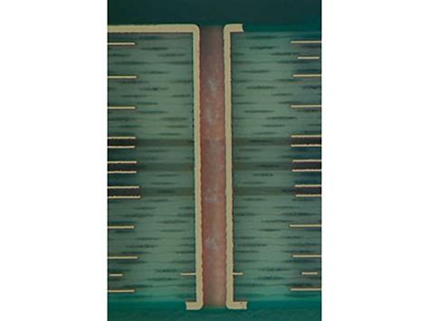
Layers in a Multilayer PCB
A typical multilayer PCB consists of the following layers:
1. Copper Layers
Copper layers are the conductive layers in a multilayer PCB, responsible for carrying electrical signals between components. The number of copper layers can vary depending on the complexity of the circuit design, ranging from four to twelve or more.
2. Insulating Layers
Insulating layers, also called prepreg (pre-impregnated) layers, are made of a non-conductive material, such as FR-4, that separates the copper layers. These layers provide electrical insulation and structural support to the PCB.
3. Solder Mask
The solder mask is a thin, protective layer applied to the outer surfaces of the PCB. It helps prevent short circuits and protects the copper traces from oxidation and damage during the soldering process.
4. Silkscreen
The silkscreen layer is a printed layer on top of the solder mask that contains text, logos, and component identifiers. This layer helps with the assembly and troubleshooting of the PCB.

Manufacturing Process of Multilayer PCBs
The manufacturing process of multilayer PCBs involves several steps:
- Design and layout
- Material preparation
- Lamination
- Drilling
- Plating
- Etching
- Solder Mask Application
- Silkscreen printing
- Surface finish application
- Electrical testing and inspection
1. Design and Layout
The first step in manufacturing a multilayer PCB is designing the circuit and creating a layout using CAD (Computer-Aided Design) software. The layout includes the placement of components, routing of traces, and the arrangement of layers.
2. Material Preparation
The required materials, such as copper foils, prepregs, and core substrates, are cut to size and prepared for lamination.
3. Lamination
The prepared layers are stacked together in the proper sequence and laminated under high temperature and pressure to create a solid, multi-layered board.
4. Drilling
Holes are drilled through the laminated board to accommodate components and vias, which are used to connect different layers.
5. Plating
The drilled holes are plated with copper to create electrical connections between layers.
6. Etching
Unwanted copper is removed from the outer layers using a chemical etching process, leaving only the desired traces.
7. Solder Mask Application
A solder mask is applied to the outer layers to protect the copper traces and prevent short circuits.
8. Silkscreen Printing
The silkscreen layer is printed onto the solder mask, providing text and identifiers for components.
9. Surface Finish Application
A surface finish, such as HASL (Hot Air Solder Leveling) or ENIG (Electroless Nickel Immersion Gold), is applied to the exposed copper areas to prevent oxidation and enhance solderability.
10. Electrical Testing and Inspection
The completed multilayer PCB undergoes electrical testing and visual inspection to ensure proper functionality and quality.

Applications of Multilayer PCBs
Multilayer PCBs find applications in various industries due to their ability to accommodate complex circuits and high component density. Some common applications include:
- Consumer electronics (smartphones, laptops, tablets)
- Automotive electronics (infotainment systems, engine control units)
- Medical devices (imaging equipment, monitoring systems)
- Aerospace and defense systems (avionics, radar)
- Industrial automation and control systems

Designing Multilayer PCBs
Designing multilayer PCBs requires careful consideration of several factors to ensure optimal performance and manufacturability. Some key aspects to consider include:
1. Layer Stack-up
The arrangement of copper and insulating layers in a multilayer PCB is called the layer stack-up. A well-designed stack-up ensures proper signal integrity, minimizes crosstalk, and reduces EMI.
2. Signal Integrity
Signal integrity refers to the quality of electrical signals transmitted through the PCB. Factors such as trace width, spacing, and impedance matching must be considered to maintain signal integrity and minimize distortion.
3. Power and Ground Planes
Dedicated power and ground planes in a multilayer PCB provide a low-impedance path for power distribution and help reduce noise and EMI.
4. Via Placement and Optimization
Vias are used to connect traces on different layers of the PCB. Proper placement and optimization of vias are crucial for maintaining signal integrity and minimizing signal reflections.
5. Design for Manufacturing (DFM)
Designing a multilayer PCB with manufacturability in mind helps reduce production costs and improve yield. DFM guidelines include minimum trace width and spacing, hole sizes, and clearances.
Challenges in Multilayer PCB Manufacturing
Manufacturing multilayer PCBs presents several challenges that must be addressed to ensure high-quality and reliable boards:
- Registration and alignment of layers
- Managing thermal expansion during lamination
- Avoiding delamination and layer separation
- Minimizing signal loss and crosstalk
- Ensuring proper hole plating and via formation
Future Trends in Multilayer PCBs
As electronic devices continue to become more compact and sophisticated, multilayer PCBs are expected to evolve to meet the growing demands. Some future trends in multilayer PCB technology include:
- Increased layer count and density
- Adoption of high-speed materials (e.g., low-loss dielectrics)
- Embedded components and 3D packaging
- Advanced manufacturing techniques (e.g., additive manufacturing)
- Integration of flexible and Rigid-Flex PCBs
Frequently Asked Questions (FAQ)
1. What is the difference between a multilayer PCB and a Single-Layer PCB?
A single-layer PCB has only one conductive layer, while a multilayer PCB has three or more conductive layers separated by insulating layers. Multilayer PCBs offer higher component density, better signal integrity, and reduced EMI compared to single-layer PCBs.
2. How many layers can a multilayer PCB have?
The number of layers in a multilayer PCB can vary depending on the complexity of the circuit design and the application requirements. Common layer counts range from four to twelve, but some advanced PCBs can have up to thirty layers or more.
3. What materials are used in multilayer PCBs?
The most common materials used in multilayer PCBs are:
- Copper foils for conductive layers
- FR-4 (Flame Retardant 4) laminate for insulating layers
- Solder mask for protective coating
- Silkscreen ink for text and identifiers
4. How are the layers connected in a multilayer PCB?
The layers in a multilayer PCB are connected through vias, which are plated holes that allow electrical signals to pass between layers. There are different types of vias, such as Through-hole vias, blind vias, and buried vias, depending on their location and connectivity within the PCB.
5. What are the advantages of using multilayer PCBs in electronic devices?
Multilayer PCBs offer several advantages in electronic devices, including:
- Higher component density, allowing for more compact and lightweight devices
- Improved signal integrity and reduced electromagnetic interference (EMI)
- Better heat dissipation and thermal management
- Increased reliability and durability
- Reduced overall system cost and improved manufacturability
Conclusion
Multilayer PCBs have revolutionized the electronics industry by enabling the design and manufacture of complex, high-density circuits in compact form factors. By understanding the structure, manufacturing process, and design considerations of multilayer PCBs, engineers and designers can create advanced electronic devices that meet the ever-growing demands of modern applications.
As technology continues to evolve, multilayer PCBs are expected to play an increasingly important role in shaping the future of electronics, from consumer gadgets to industrial automation and beyond.
Leave a Reply