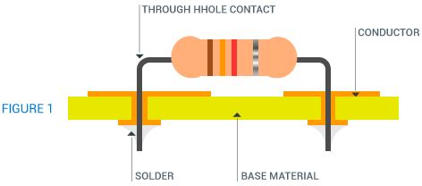
What is Through-hole Assembly?
Through-hole assembly is a method of mounting electronic components on a printed circuit board (PCB) by inserting the component leads through holes drilled in the board and soldering them to pads on the opposite side. This technique has been widely used since the early days of electronics manufacturing and remains a reliable and cost-effective option for many applications, despite the growing popularity of Surface-Mount Technology (SMT).
Advantages of Through-hole Assembly
- Mechanical strength: Through-hole components provide a stronger mechanical connection to the PCB compared to surface-mount components, making them more resistant to vibration and physical stress.
- Ease of manual assembly: Through-hole components are easier to handle and solder manually, making them suitable for prototyping, low-volume production, and hobbyist projects.
- Visual inspection: Solder joints in through-hole assembly are visible on the opposite side of the PCB, allowing for easier visual inspection and troubleshooting.
- Higher power handling: Through-hole components can often handle higher power levels than their surface-mount counterparts due to their larger size and better heat dissipation.
Disadvantages of Through-hole Assembly
- Board space: Through-hole components occupy more PCB space compared to surface-mount components, limiting the potential for miniaturization.
- Higher cost: Drilling holes in the PCB and the larger size of through-hole components can increase manufacturing costs, especially for high-volume production.
- Limited component availability: As surface-mount technology becomes more prevalent, some components may only be available in SMT packages, limiting design options for through-hole assembly.
Through-hole Assembly Process
The through-hole assembly process consists of several steps, each of which is crucial for ensuring a reliable and high-quality end product.
1. PCB Design and Fabrication
The first step in through-hole assembly is designing the PCB layout, which includes determining the component placement, routing the traces, and creating the necessary holes for through-hole components. The design is then sent to a PCB fabrication facility, where the board is manufactured according to the specified design.
2. Component Preparation
Before the assembly process can begin, the through-hole components must be prepared for insertion. This may involve:
- Lead forming: Bending the component leads to fit the hole spacing on the PCB.
- Tape and reel packaging: Placing components on a carrier tape for automated insertion.
- Kit packaging: Grouping components together for manual assembly.
3. Component Insertion
Once the components are prepared, they are inserted into the appropriate holes on the PCB. This can be done manually or using automated insertion machines, depending on the production volume and available resources.
- Manual insertion: Operators manually place components into the PCB holes, ensuring the correct orientation and fit.
- Automated insertion: Machines, such as axial and radial insertion machines, automatically place components into the PCB holes at a high speed and with great precision.
4. Soldering
After the components are inserted, the PCB undergoes the soldering process to create a permanent electrical and mechanical connection between the component leads and the PCB pads.
- Wave soldering: The PCB is passed over a molten solder wave, which contacts the component leads and PCB pads, creating a solder joint.
- Selective soldering: A targeted soldering process that applies solder only to specific areas of the PCB, useful for boards with a mix of through-hole and surface-mount components.
- Hand soldering: Operators manually solder the component leads to the PCB pads using a soldering iron, often used for prototyping or low-volume production.
5. Inspection and Testing
Once the soldering process is complete, the PCB undergoes inspection and testing to ensure the quality and functionality of the assembled board.
- Visual inspection: Operators or automated optical inspection (AOI) systems check for visible defects, such as missing components, incorrect orientation, or poor solder joints.
- Electrical testing: The assembled PCB is tested for electrical continuity, short circuits, and overall functionality using various test methods, such as in-circuit testing (ICT) or functional testing.
6. Rework and Repair
If any defects or issues are identified during the inspection and testing phase, the PCB may require rework or repair. This involves:
- Desoldering: Removing the faulty component or solder joint using desoldering tools, such as a desoldering pump or solder wick.
- Replacement: Installing a new component or resoldering the joint to correct the issue.
- Re-testing: Verifying that the rework or repair has resolved the problem and the PCB functions as intended.

Through-hole Component Types
Through-hole assembly accommodates a wide range of component types, each with its own characteristics and applications.
Resistors
Resistors are passive components that limit the flow of electric current in a circuit. Through-hole resistors are available in various packages, such as axial and radial lead configurations, and are commonly used in power circuits, voltage dividers, and pull-up/pull-down networks.
| Package Type | Power Rating | Resistance Range | Applications |
|---|---|---|---|
| Axial lead | 1/8W – 2W | 0.1Ω – 10MΩ | General purpose, power circuits |
| Radial lead | 1/4W – 5W | 0.1Ω – 100MΩ | High power, heat sinks |
Capacitors
Capacitors are passive components that store electric charge and are used for filtering, coupling, and decoupling in electronic circuits. Through-hole capacitors come in various dielectric materials, such as ceramic, film, and electrolytic, each with different properties and applications.
| Dielectric Material | Capacitance Range | Voltage Range | Applications |
|---|---|---|---|
| Ceramic | 1pF – 10µF | 10V – 500V | High-frequency, general purpose |
| Film | 1nF – 10µF | 50V – 1000V | Audio, power supply filtering |
| Electrolytic | 1µF – 10,000µF | 6.3V – 450V | Power supply filtering, coupling |
Inductors
Inductors are passive components that store energy in a magnetic field and are used for filtering, energy storage, and impedance matching. Through-hole inductors are available in various core materials, such as air, ferrite, and iron, and can be found in different package types, like radial and axial lead configurations.
| Core Material | Inductance Range | Current Rating | Applications |
|---|---|---|---|
| Air | 1nH – 100µH | 10mA – 1A | High-frequency, low-power |
| Ferrite | 1µH – 10mH | 100mA – 5A | EMI suppression, power conversion |
| Iron | 1mH – 100H | 100mA – 10A | Low-frequency, high-power |
Diodes
Diodes are semiconductor components that allow current to flow in only one direction and are used for rectification, protection, and switching. Through-hole diodes come in various types, such as signal, rectifier, and Zener diodes, each with specific characteristics and applications.
| Diode Type | Forward Voltage | Reverse Voltage | Applications |
|---|---|---|---|
| Signal | 0.3V – 0.7V | 50V – 200V | Switching, clamping |
| Rectifier | 0.6V – 1.2V | 50V – 1000V | Power rectification, voltage doubling |
| Zener | 1.8V – 200V | 1.8V – 200V | Voltage regulation, protection |
Transistors
Transistors are semiconductor components used for amplification and switching in electronic circuits. Through-hole transistors are available in different types, such as bipolar junction transistors (BJTs) and field-effect transistors (FETs), and can be found in various package types, like TO-92 and TO-220.
| Transistor Type | Gain (hFE) | Frequency Range | Applications |
|---|---|---|---|
| BJT (NPN, PNP) | 50 – 1000 | DC – 500MHz | Amplification, switching |
| MOSFET (N, P) | 1 – 1000 | DC – 10GHz | Power switching, RF amplification |
| JFET (N, P) | 1 – 100 | DC – 1GHz | Low-noise amplification, switching |
Integrated Circuits
Integrated circuits (ICs) are miniaturized electronic circuits that combine multiple components, such as transistors, diodes, and resistors, on a single semiconductor substrate. Through-hole ICs come in various package types, like DIP (Dual In-line Package) and SIP (Single In-line Package), and are used for a wide range of applications, from simple logic functions to complex microcontrollers and processors.
| Package Type | Pin Count | Pitch | Applications |
|---|---|---|---|
| DIP | 8 – 64 | 0.1″ | General purpose, microcontrollers |
| SIP | 4 – 32 | 0.1″ | Memory, power supplies |
| TO-220 | 3 – 7 | 0.2″ | Voltage regulators, power amplifiers |

Through-hole Assembly Best Practices
To ensure high-quality and reliable through-hole assembly, consider the following best practices:
- Design for manufacturability (DFM): Adhere to industry-standard design guidelines, such as hole sizes, pad dimensions, and component spacing, to facilitate efficient and accurate assembly.
- Component selection: Choose components with appropriate ratings, packages, and lead configurations for the intended application and assembly process.
- Solder paste and flux: Select solder paste and flux that are compatible with the PCB material, component finishes, and soldering process to achieve optimal solder joint quality.
- Process control: Monitor and control key process parameters, such as solder temperature, dwell time, and insertion force, to maintain consistency and prevent defects.
- Inspection and testing: Implement a robust inspection and testing strategy, including visual inspection, automated optical inspection (AOI), and electrical testing, to identify and address defects early in the assembly process.
- Rework and repair: Establish clear procedures and guidelines for rework and repair, including proper tools, techniques, and documentation, to ensure the integrity of the repaired assembly.
- Continuous improvement: Regularly review and analyze assembly process data, identify areas for improvement, and implement corrective actions to enhance quality, efficiency, and reliability.

Frequently Asked Questions (FAQ)
- What is the difference between through-hole and surface-mount assembly?
-
Through-hole assembly involves inserting component leads through holes drilled in the PCB and soldering them to pads on the opposite side, while surface-mount assembly involves placing components directly onto pads on the surface of the PCB and soldering them in place.
-
Can through-hole and surface-mount components be used together on the same PCB?
-
Yes, mixed-technology PCBs that combine through-hole and surface-mount components are common in many applications. However, the assembly process may require additional steps, such as selective soldering, to accommodate the different component types.
-
What are the most common defects in through-hole assembly, and how can they be prevented?
-
Common defects in through-hole assembly include poor solder joints, component misalignment, and missing or damaged components. These defects can be prevented by following best practices in design, component selection, process control, and inspection.
-
How does the hole size affect the through-hole assembly process?
-
The hole size should be appropriate for the component lead diameter and the soldering process. Holes that are too small can make component insertion difficult and lead to poor solder joints, while holes that are too large can result in inadequate solder fill and weak mechanical connections.
-
What are the environmental considerations for through-hole assembly?
- Through-hole assembly processes, particularly soldering, can involve the use of lead-based solders and fluxes that may have environmental and health implications. It is important to consider using lead-free solders and environmentally friendly fluxes, as well as implementing proper ventilation and waste management practices to minimize the environmental impact of the assembly process.
Leave a Reply