What is Solder Mask and Why is it Important?
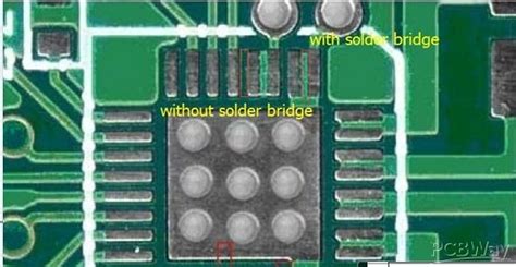
Solder mask, also known as solder resist or solder stop, is a thin layer of polymer applied to the copper traces of a printed circuit board (PCB). Its primary purpose is to protect the copper traces from oxidation, prevent solder bridges from forming between closely spaced pads, and provide electrical insulation. Solder mask also serves as a barrier against environmental contaminants and improves the overall durability of the PCB.
The application of solder mask is a critical step in the PCB manufacturing process, as it directly impacts the quality, reliability, and functionality of the final product. A well-applied solder mask ensures that the PCB will function as intended and withstand the rigors of its intended application.
Solder Mask Application Methods
There are several methods for applying solder mask to a PCB, each with its own advantages and disadvantages. The choice of method depends on factors such as the desired finish, the complexity of the PCB design, and the production volume. The most common solder mask application methods are:
Screen Printing
Screen printing is the most widely used method for applying solder mask to PCBs. It involves using a fine mesh screen with a Stencil of the desired solder mask pattern. The solder mask ink is pushed through the screen onto the PCB surface using a squeegee. The PCB is then cured in an oven to harden the solder mask.
Advantages of screen printing include:
– Cost-effective for high-volume production
– Suitable for a wide range of solder mask materials
– Produces a consistent and uniform coating
Disadvantages of screen printing include:
– Limited resolution compared to other methods
– Requires frequent screen cleaning and maintenance
– Not suitable for complex PCB designs with fine features
Liquid Photo Imaging (LPI)
Liquid Photo Imaging (LPI) is a high-resolution solder mask application method that uses a photosensitive liquid solder mask. The PCB is coated with the liquid solder mask, and then a photographic film with the desired solder mask pattern is placed on top. The PCB is exposed to UV light, which cures the exposed areas of the solder mask. The unexposed areas are then removed using a developer solution.
Advantages of LPI include:
– High resolution and accuracy
– Suitable for complex PCB designs with fine features
– Produces a smooth and uniform surface finish
Disadvantages of LPI include:
– More expensive than screen printing
– Requires specialized equipment and materials
– Longer processing time compared to screen printing
Dry Film Solder Mask
Dry film solder mask is a solid, photosensitive film that is laminated onto the PCB surface using heat and pressure. The film is then exposed to UV light through a photographic film with the desired solder mask pattern. The unexposed areas are removed using a developer solution, leaving the cured solder mask on the PCB.
Advantages of dry film solder mask include:
– High resolution and accuracy
– Suitable for complex PCB designs with fine features
– Faster processing time compared to LPI
Disadvantages of dry film solder mask include:
– More expensive than screen printing
– Requires specialized equipment and materials
– Limited flexibility compared to liquid solder masks

Solder Mask Application Process
Regardless of the chosen application method, the solder mask application process generally follows these steps:
-
PCB Cleaning: The PCB surface is thoroughly cleaned to remove any dirt, grease, or oxidation that could affect the adhesion of the solder mask.
-
Solder Mask Application: The solder mask is applied to the PCB using one of the methods described above (screen printing, LPI, or dry film).
-
Curing: The solder mask is cured using heat, UV light, or a combination of both, depending on the type of solder mask material used. Curing hardens the solder mask and ensures its adherence to the PCB surface.
-
Inspection: The PCB is inspected for any defects in the solder mask, such as pinholes, bubbles, or uneven coverage. Automated Optical Inspection (AOI) systems are often used to detect and analyze these defects.
-
Touch-up and Repair: If any defects are found during the inspection, they are corrected using manual touch-up or repair techniques. This may involve applying additional solder mask material or removing excess material.
-
Final Curing: After any necessary touch-ups or repairs, the PCB undergoes a final curing process to ensure the solder mask is fully hardened and adhered to the surface.

Solder Mask Materials
Solder mask materials are typically epoxy or acrylic-based polymers that are formulated to provide excellent electrical insulation, chemical resistance, and thermal stability. The choice of solder mask material depends on the specific requirements of the PCB, such as the operating environment, the desired color, and the compatibility with the chosen application method.
Some common solder mask materials include:
-
Liquid Photoimageable Solder Mask (LPISM): A photosensitive liquid solder mask that is applied using the LPI method. LPISM offers high resolution and a smooth surface finish.
-
Dry Film Photoimageable Solder Mask (DFISM): A photosensitive film solder mask that is applied using the dry film method. DFISM provides high resolution and fast processing times.
-
Epoxy Liquid Solder Mask: A two-part epoxy-based liquid solder mask that is applied using the screen printing method. Epoxy liquid solder mask offers excellent chemical resistance and durability.
-
Acrylic Liquid Solder Mask: A one-part acrylic-based liquid solder mask that is applied using the screen printing method. Acrylic liquid solder mask provides good electrical insulation and is available in a wide range of colors.

Solder Mask Colors
Solder mask is available in a variety of colors, with green being the most common. The choice of color is often dictated by the specific application or industry standards. For example, blue solder mask is often used in the medical device industry, while red solder mask is common in the aerospace industry.
Some popular solder mask colors include:
| Color | Pantone Code | RAL Code | Application |
|---|---|---|---|
| Green | 356 C | 6018 | Most common, general-purpose |
| Blue | 2935 C | 5015 | Medical devices, high-reliability |
| Red | 185 C | 3020 | Aerospace, military |
| Yellow | 123 C | 1018 | High-visibility, warning labels |
| Black | Black C | 9005 | High-contrast, aesthetic purposes |
| White | White C | 9003 | LED lighting, reflective surfaces |
Frequently Asked Questions (FAQ)
-
What is the difference between solder mask and conformal coating?
Solder mask is applied to the PCB surface before the components are soldered, and it serves to protect the copper traces and prevent solder bridges. Conformal coating, on the other hand, is applied after the components are soldered and provides additional protection against moisture, dust, and other environmental factors. -
Can solder mask be removed?
Yes, solder mask can be removed using various methods, such as mechanical abrasion, chemical etching, or laser ablation. However, removing solder mask should only be done when absolutely necessary, as it can damage the underlying copper traces and compromise the integrity of the PCB. -
How does solder mask affect the soldering process?
Solder mask helps to control the flow of solder during the soldering process by defining the areas where solder should be applied (exposed pads) and the areas where it should not (covered traces). This prevents solder bridges from forming between closely spaced pads and ensures a reliable and consistent solder joint. -
What is the typical thickness of solder mask?
The typical thickness of solder mask ranges from 0.5 to 2.0 mils (0.0127 to 0.0508 mm), depending on the application method and the specific requirements of the PCB. A thicker solder mask provides better insulation and protection but may affect the fine-pitch component placement. -
Can solder mask be used on Flexible PCBs?
Yes, solder mask can be applied to flexible PCBs using specialized materials and application methods. Flexible solder masks are formulated to withstand the bending and flexing of the PCB without cracking or peeling. They are typically applied using screen printing or photoimaging techniques adapted for flexible substrates.
Conclusion
Solder mask application is a critical step in the PCB manufacturing process, ensuring the protection, insulation, and reliability of the copper traces. The choice of application method, material, and color depends on the specific requirements of the PCB and the intended application. By understanding the various aspects of solder mask application, PCB designers and manufacturers can make informed decisions to optimize the performance and durability of their products.
As PCB technology continues to evolve, so do the solder mask materials and application methods. Advanced solder mask formulations and application techniques are being developed to meet the demands of increasingly complex and miniaturized PCB designs. These include high-temperature solder masks for lead-free soldering processes, direct imaging solder masks for ultra-fine pitch components, and environmentally friendly solder mask materials that comply with global sustainability standards.
Ultimately, the successful application of solder mask is a collaborative effort between PCB designers, manufacturers, and material suppliers. By working together to select the most appropriate solder mask solution for each project, they can ensure the highest quality and reliability of the final PCB product.
Leave a Reply