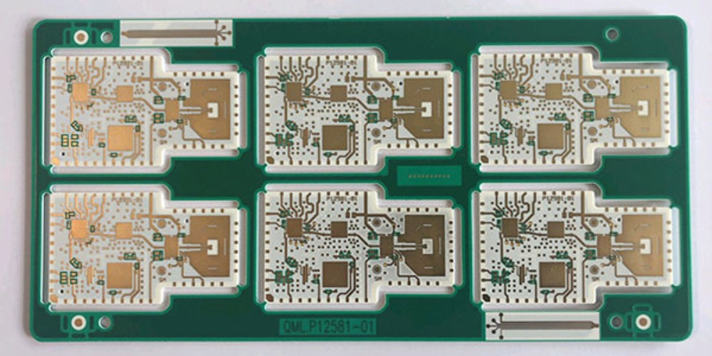
Overview of RF Shielding for PCBs
Radio frequency (RF) interference can disrupt the operation of electronic circuits and degrade signal integrity. Proper RF shielding techniques are essential for protecting sensitive PCB components from electromagnetic interference (EMI). This article provides an overview of common RF shielding methods used during PCB design and manufacturing.
Importance of RF Shielding
RF shielding prevents electromagnetic fields from radiating outwards or inwards. Key benefits include:
- Reduces cross-talk between components and circuits
- Limits emission of EMI to meet regulatory compliance
- Improves signal quality by blocking external interference
- Enables operation of multiple wireless technologies in close proximity
Proper RF shielding is critical for PCBs used in telecommunications, IoT devices, aerospace systems, and automotive electronics.
RF Shielding Techniques for PCBs

There are various options available for shielding a PCB from RF interference:
Shield Cans
Metal shield cans placed over individual components or sections of a PCB are commonly used. They block EMI through reflection and absorption. Various types are available based on form factors needed:
- Box-type enclosures
- Clam-shell enclosures
- Square or rectangular covers
- Flexible gasketed screens
Shield cans are suitable for shielding medium to large components. Drawbacks include increased weight and cost.
Board Level Shields
Prefabricated metal shields adhered directly to the PCB surface provide RF isolation. Popular options are:
- Adhesive copper tape – Low cost but less durable
- Plated metal-polymer composite shields – Good thermal/electrical performance
- Soldered metal clip-on shields – Reusable but high cost
- Conformal coatings – Lightweight but limited attenuation
Board level shields integrate easily without much increase in height. Performance can vary based on type used.
Embedded Shielding
Shielding can be embedded within the PCB stackup:
- Ground planes – Provide continuous shielding and enclosure
- Buried metal layers – Localized shielding underneath components
- Plated through-hole vias – Form a Faraday cage around components
Embedded shielding is lightweight and cost-effective. Design constraints include PCB layer count and component height restrictions.
EMI Gaskets
Conductive elastomer gaskets are used along joints and seams between metal shields. They prevent leakage of EMI through gaps. Common types are:
- Conductive foam strips
- Woven wire mesh
- Oriented wire gaskets
- Spring finger gaskets
Gaskets compensate for poor fit between shields and ensure electrical continuity.
Best Practices for PCB RF Shielding
To maximize shielding effectiveness, the following guidelines should be followed:
- Enclose components in contiguous metallic shields
- Minimize openings and seams
- Use multiple small openings instead of large openings
- Treat seams and joints with EMI gaskets
- Use plated through-hole vias as “Via Fences” around components
- Connect all shields to low impedance ground plane
- Extend shielding beyond wavelength of highest noise frequency
- Follow a systematic shielding hierarchy for sub-systems
Careful design is needed to balance shielding performance and cost trade-offs.
Testing Shielding Effectiveness
Shielding performance should be validated through laboratory testing:
- Radiated emissions testing checks for any leakage
- Antenna isolation testing measures susceptibility
- Optical fibers can map leakage points during testing
Any shielding deficiencies can then be addressed through design improvements.
Conclusion
With rising EMI issues, RF shielding is now essential in most PCBs. The shielding method can be selected based on frequency range, cost, weight, manufacturability, and other factors. A combination of different techniques may be required. Early consideration of shielding requirements during the design phase is highly recommended.
FQA
Q: What are the typical frequencies used in RF shielding for PCBs?
A: Common RF frequencies requiring shielding for PCBs range from 10 MHz up to 10 GHz, including applications like cellular, WiFi, Bluetooth, GPS, and radio communications. Higher frequencies up to 100 GHz may also need shielding in some cases.
Q: How much attenuation can be achieved with RF shields?
A: Typical shielding effectiveness values range from 40 dB to 100 dB depending on the shielding method used. Greater than 60-80 dB attenuation is considered very effective shielding for most applications.
Q: What is the importance of grounding in RF shielding?
A: For any shielding enclosure to be effective, it has to be properly grounded to a low impedance return path, usually the ground plane. Improper grounding can impair performance and even create additional EMI leakage.
Q: Can multiple ground layers help improve RF shielding?
A: Having multiple continuous ground plane layers in the PCB stackup helps increase shielding effectiveness. The ground planes act as embedded shields surrounding components and routing signals.
Q: How are openings and seams handled when designing shielded enclosures?
A: Openings and seams in shielded enclosures can allow EMI leakage. Small openings less than 1/10th wavelength will not degrade shielding. Larger openings may need conductive gaskets. Overlapping seams is also recommended.
Leave a Reply