Introduction
Printed circuit boards (PCBs) are essential components in microwave systems like radar, wireless communications, and satellite broadcasting. The increasing demand for higher frequencies and bandwidths puts stringent requirements on microwave PCBs. Proper design is crucial for good microwave performance and reliability. This article discusses key factors in microwave PCB design.
Material Selection
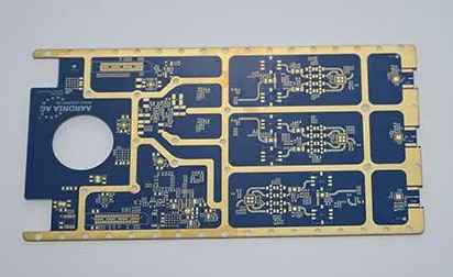
The substrate material significantly impacts the electrical performance of a microwave PCB. Important parameters are dielectric constant (DK), loss tangent, and thermal properties. Standard FR-4 is unsuitable above a few GHz due to high losses. Common microwave materials include:
- PTFE composites like Rogers RO4000 series – low loss, stable DK.
- Ceramic filled PTFE – lower cost than PTFE, higher loss.
- High frequency laminates like Rogers RO3000 series – glass microfiber filled PTFE, balanced electrical and thermal properties.
Selecting the right material depends on frequency, loss, thermal, and cost requirements.
Trace Geometry

Controlling trace geometry is vital for good impedance control and low radiation losses. Key factors are:
- Trace width – determines characteristic impedance along with substrate DK.
- Trace thickness – thicker traces have lower losses but take up more space.
- Edge couping – can increase impedance for narrow traces.
- Vias – need low inductance for good grounding, avoid stubs.
Use a stackup with thicker outer layers for low loss transmission lines. Minimize bends and maintain clearance between traces to control crosstalk.
Grounding and Shielding
Proper system grounding is essential for directing return currents and suppressing noise coupling. A continuous ground plane underneath traces is ideal. Multiple vias connect the ground planes. Shielding sensitive traces can reduce coupling. Avoid slots or gaps in ground structures.
Component Selection
Passive components like capacitors and resistors must also work well at microwave frequencies. Identify suitable RF-rated components and ensure they are properly grounded and isolated. Mount them close to the devices they connect to minimize parasitic inductance.
Transitions and Discontinuities
Impedance mismatches at transitions between transmission lines or at component discontinuities cause reflections which degrade performance. Use tapers, steps, or matching networks to improve matching. Eliminate unwanted discontinuities. Simulations help identify problem areas.
Modeling and Simulation
Modern EM simulation helps accurately model microwave structures, fields, and performance. This improves designs by identifying issues before fabrication. Simulate transmission lines, discontinuities, radiation, and coupling effects. Vendor supplied models aid component selection.
Fabrication Considerations
Many fabrication factors affect microwave PCB performance like dielectric thickness, conductor profile, lamination pressure, and more. Work with the board shop to control critical parameters and to get accurate material data for simulations. Follow their design rules.
Testing
Test microwave PCBs thoroughly to validate the design. Network analyzer measurements like insertion loss, return loss, and group delay characterize performance. Additional environmental stress screening is recommended. Update the design as needed based on results.
Conclusion
Microwave PCB development requires specialized design expertise. Paying attention to aspects like material selection, controlled impedances, grounding, and modeling results in reliable high-frequency performance. Work closely with fabrication partners to achieve success.
Frequently Asked Questions
Q1. What are some typical microwave PCB substrate materials?
Some common microwave PCB substrate materials are PTFE composites like Rogers RO4000 series, ceramic filled PTFE, and glass microfiber filled PTFE laminates like Rogers RO3000 series. The substrate choice depends on the frequency range, loss, thermal, and cost requirements.
Q2. How can discontinuities be minimized in a microwave PCB design?
Discontinuities can be minimized through careful layout by avoiding abrupt stubs and bends in transmission lines. Where discontinuities are unavoidable, use mitigation techniques like tapers, steps, or matching networks to improve impedance matching and reduce reflections. Simulations help identify problem areas.
Q3. What are some techniques to reduce crosstalk in microwave PCBs?
Maintaining adequate spacing between traces reduces coupling between them. A continuous ground plane underneath the traces confines fields and reduces crosstalk. Selective shielding of sensitive traces and avoidance of slots or gaps in ground planes also helps suppress coupling. Terminating traces helps damp resonances.
Q4. Why is it important to model and simulate microwave PCBs?
Modeling and simulation are important to accurately characterize microwave effects like impedance, coupling, radiation losses, and resonances. This allows issues to be identified and addressed early in the design phase before committing to fabrication. Access to accurate substrate data and component models is key.
Q5. How are microwave PCBs tested during fabrication and after completion?
During fabrication, coupon testing helps characterize materials properties. Completed boards are tested using network analyzers to measure parameters like insertion loss, return loss, and group delay. Additional environmental stress screening for vibration, temperature cycling etc. may be warranted. Results guide design improvements.
Leave a Reply