What is a PCB Prototype?
A PCB prototype, short for printed circuit board prototype, is an early sample or model of a PCB used for testing and evaluation purposes before mass production. Creating prototypes is an essential part of the electronics design process. It allows engineers to test the functionality, find design flaws, verify the PCB layout, and make necessary revisions prior to manufacturing the final product.
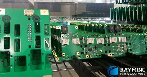
PCB prototypes are typically fabricated in small quantities, sometimes even as a single unit, using quick-turn or rapid PCB prototyping services. The prototypes closely match the final product in terms of material, layer count, component placement, and features, but may not have the final surface finish or soldermask.
Advantages of PCB Prototyping
Creating PCB prototypes offers several key advantages in the product development process:
- Design Validation: Prototypes allow you to test your PCB design in the real world, outside of computer simulations. You can verify the functionality, signal integrity, power distribution, and other critical aspects of your design.
- Finding Flaws Early: Identifying and fixing design issues early in the prototyping phase is much less costly than discovering problems after mass production has begun. Prototyping helps you iterate and refine your design.
- Testing Compatibility: You can test how well your PCB integrates with other components, enclosures, or systems it needs to interface with. Any compatibility issues can be ironed out during prototyping.
- Demonstrating Proof of Concept: A working prototype proves the viability of your design to stakeholders, investors, or customers. It demonstrates your concept better than schematics or computer models.
- Faster Time to Market: Thorough prototyping leads to a more robust final product and helps avoid costly redesigns or production delays. It streamlines the path from idea to finished product.
PCB Prototyping Process
The PCB prototyping process typically involves the following steps:
- Design: Create your schematic and PCB layout using EDA (Electronic Design Automation) software. Carefully select your components, define your stackup, and lay out your board according to design rules and manufacturing constraints.
- Design Rule Check (DRC): Run a DRC on your PCB layout to catch any errors or rule violations, such as trace spacing issues, insufficient annular rings, or silk screen overlaps. Make necessary corrections.
- Generate Manufacturing Files: Export the required files for manufacturing, typically Gerber files and drill files. Include any additional fabrication or assembly notes.
- Select a PCB Manufacturer: Choose a PCB manufacturer or quick-turn PCB prototyping service based on your requirements for turnaround time, quality, pricing, and capabilities.
- Place Your Order: Upload your manufacturing files and place your order, specifying any special requirements such as surface finish, soldermask color, or controlled impedance.
- PCB Fabrication: Your PCB prototypes are fabricated according to your specifications. Quick-turn prototyping services can often produce boards in 24 to 48 hours.
- Assembly (optional): If required, your PCB prototypes can be assembled with components, either by the PCB manufacturer or a separate assembly house.
- Testing and Evaluation: Once you receive your prototypes, thoroughly test and evaluate them. Verify functionality, take measurements, and look for any issues or areas for improvement.
- Revisions: Based on your evaluation, make any necessary revisions to your design. You may need to go through multiple iterations of prototyping until you achieve your desired results.
- Final Production: Once your design is finalized and validated through prototyping, you can proceed with mass production of your PCB.

Choosing a PCB Prototyping Service
When selecting a PCB prototyping service, consider the following factors:
- Capabilities: Ensure the service can handle your specific requirements for PCB size, layer count, materials, surface finishes, and special features like controlled impedance or blind/buried vias.
- Turnaround Time: If you need your prototypes quickly, look for services offering express or same-day turnaround options. Keep in mind that faster turnaround times often come at a higher cost.
- Quality: Check the service’s reputation for quality and reliability. Look for certifications like ISO 9001, UL listing, or IPC class standards. Read reviews or ask for recommendations from other engineers.
- Pricing: Get quotes from multiple services and compare pricing, but don’t sacrifice quality for the lowest price. Consider the total cost, including any setup fees, tooling charges, or shipping costs.
- Design Support: Some services offer design assistance, such as DFM (Design for Manufacturability) feedback or design rule checking. This can be helpful if you’re less experienced with PCB design.
- Assembly Options: If you need your prototypes assembled, look for services that offer turnkey assembly or can recommend reliable assembly partners.
- Communication and Support: Choose a service with responsive customer support and clear communication channels. They should be able to answer your questions and keep you updated on the status of your order.
Popular PCB Prototyping Services
Here are some popular PCB prototyping services known for their capabilities and quick turnaround times:
| Service | Capabilities | Turnaround Time |
|---|---|---|
| PCBWay | Up to 16 layers, various materials and finishes | Standard 3-5 days, expedited 24-48 hours |
| OSH Park | Up to 6 layers, unique purple soldermask | Standard 12-14 days, expedited 5 days |
| Seeed Studio | Up to 16 layers, flexible and rigid-flex options | Standard 5-7 days, expedited 3-4 days |
| JLCPCB | Up to 6 layers, aluminum PCBs, assembly service | Standard 5-7 days, expedited 24-48 hours |
| Advanced Circuits | Up to 32 layers, high-density interconnect | Standard 5-7 days, expedited 2-3 days |

Tips for Successful PCB Prototyping
To ensure a smooth and successful PCB prototyping process, follow these tips:
- Design for Manufacturability (DFM): Adhere to the design rules and guidelines provided by your PCB manufacturer. This includes minimum trace widths, clearances, drill sizes, and annular ring requirements. Designing with manufacturability in mind reduces the risk of fabrication issues.
- Use a Template: Many PCB manufacturers provide templates or design rule files for their specific capabilities. Using these templates from the start ensures your design is compatible with their processes.
- Choose the Right Layer Count: Determine the appropriate number of layers for your design based on complexity, routing density, and signal integrity requirements. More layers provide more routing flexibility but also increase cost.
- Select Appropriate Components: When choosing components for your prototype, consider their availability, lead time, and minimum order quantities. Avoid using hard-to-find or obsolete components that could delay your prototyping process.
- Plan Your Stackup: Carefully plan your PCB stackup, taking into account your desired impedance, dielectric thickness, and manufacturing capabilities. Consult with your manufacturer for recommendations on material selection and layer arrangement.
- Optimize Your Layout: Optimize your PCB layout for signal integrity, power distribution, and thermal management. Minimize crosstalk, avoid long parallel traces, and use appropriate grounding techniques. Consider the placement of decoupling capacitors and power planes.
- Review and Double-Check: Before submitting your design for manufacturing, thoroughly review your schematics, layout, and manufacturing files. Double-check for any errors, inconsistencies, or missing information.
- Communicate with Your Manufacturer: Maintain clear communication with your PCB manufacturer throughout the prototyping process. Provide them with any additional information, clarify any questions they may have, and respond promptly to their requests.
- Test Thoroughly: When you receive your prototypes, perform thorough testing and evaluation. Test all functions, measure critical parameters, and stress-test your design under various conditions. Document any issues or areas for improvement.
- Iterate and Refine: Based on your testing results, make necessary revisions and improvements to your design. Don’t be afraid to go through multiple iterations of prototyping until you achieve the desired performance and reliability.

FAQ
How much does PCB prototyping cost?
The cost of PCB prototyping varies depending on factors such as the size of the PCB, number of layers, materials, surface finish, quantity, and turnaround time. Many prototyping services offer discounts for larger quantities or provide low-cost options for simple 2-layer designs. As an example, a small 2-layer PCB prototype may cost around $10-30 per board, while a more complex 6-layer design may cost $50-100 per board.
How long does PCB prototyping take?
The turnaround time for PCB prototyping depends on the service you choose and the complexity of your design. Standard lead times for prototyping services range from 5 to 14 days, but many services offer expedited options for faster turnaround. Some quick-turn services can produce simple PCB prototypes in as little as 24 to 48 hours, while more complex designs may take 3 to 5 days.
What files do I need to submit for PCB prototyping?
To have your PCB prototypes manufactured, you typically need to submit Gerber files and drill files. Gerber files are the industry standard for PCB fabrication and include information about the copper layers, soldermask, silkscreen, and other features of your PCB. Drill files specify the location, size, and type of holes to be drilled in your board. Some manufacturers may also accept other file formats like ODB++ or IPC-2581.
Can I get my PCB prototypes assembled?
Yes, many PCB prototyping services offer assembly options, either in-house or through partnerships with assembly houses. You can provide your own components or have the service source them for you. Assembly options may include through-hole, surface mount, or mixed technology. If you require assembly, make sure to choose a service that can accommodate your specific needs and provide them with the necessary assembly files, such as pick and place files and bill of materials (BOM).
What should I do if I find issues with my PCB prototypes?
If you discover issues or problems with your PCB prototypes during testing and evaluation, document them carefully. Identify the root cause of each issue, whether it’s a design flaw, manufacturing defect, or assembly problem. Work with your PCB prototyping service to address any manufacturing or assembly-related issues. For design-related problems, make the necessary revisions to your schematics and layout. Then, generate updated manufacturing files and order a new set of prototypes for further testing. Repeat this process until you achieve a fully functional and reliable PCB design.
Conclusion
PCB prototyping is a crucial step in the electronics design process, allowing you to validate your designs, catch issues early, and ensure the functionality and reliability of your final product. By selecting the right PCB prototyping service, following design best practices, and thoroughly testing your prototypes, you can streamline your development process and bring your products to market faster.
Many PCB prototyping services offer free or low-cost options for creating prototypes, making it accessible for designers and engineers to iterate and refine their designs. By taking advantage of these services and following the tips outlined in this article, you can effectively prototype your PCBs and create successful electronic products.
Leave a Reply