Introduction to PCB DFM
PCB DFM (Design for Manufacturing) is a crucial aspect of PCB design that focuses on optimizing the design to ensure efficient and cost-effective manufacturing. By considering DFM guidelines during the design phase, designers can minimize potential manufacturing issues, reduce costs, and improve the overall quality of the PCB.
Key Aspects of PCB DFM
- Component Selection and Placement
- Trace Routing and Spacing
- Soldermask and Silkscreen
- Testability and Inspection
- Panelization and Fabrication
Component Selection and Placement
Choosing the Right Components
When selecting components for your PCB design, consider the following factors:
- Availability and lead time
- Cost and minimum order quantity (MOQ)
- Package size and pitch
- Thermal requirements
- Reliability and quality
Component Placement Guidelines
Proper component placement is essential for DFM. Follow these guidelines:
- Group similar components together
- Place components on a single side when possible
- Avoid placing components too close to board edges
- Consider component orientation for easier assembly
- Provide adequate spacing between components
| Component Pitch | Minimum Spacing |
|---|---|
| ≥ 0.65 mm | 0.15 mm |
| 0.5 mm – 0.65 mm | 0.1 mm |
| < 0.5 mm | 0.05 mm |

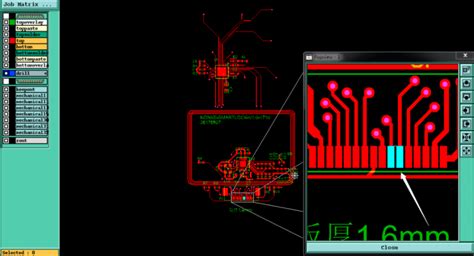
Trace Routing and Spacing
Trace Width and Spacing
When routing traces on your PCB, consider the following:
- Use appropriate trace widths based on current requirements
- Maintain adequate spacing between traces to avoid short circuits
- Follow manufacturer’s recommendations for trace width and spacing
| Current (A) | Trace Width (mm) |
|---|---|
| 0.1 | 0.15 |
| 0.5 | 0.3 |
| 1 | 0.6 |
| 2 | 1.0 |
Vias and Through-Holes
- Use appropriate via sizes based on the required current carrying capacity
- Avoid placing vias under components when possible
- Ensure proper spacing between vias and other features

Soldermask and Silkscreen
Soldermask Design
- Provide adequate soldermask expansion around pads
- Avoid soldermask between closely spaced pads
- Use appropriate soldermask color (green is most common)
Silkscreen Design
- Use clear and legible font sizes for component designators
- Avoid placing silkscreen over pads or vias
- Ensure proper alignment of silkscreen with components

Testability and Inspection
Design for Testing (DFT)
- Include test points for critical signals
- Provide clear probe access to test points
- Consider using boundary scan testing for complex designs
Automated Optical Inspection (AOI)
- Ensure adequate contrast between components and PCB surface
- Avoid using reflective surfaces that may interfere with AOI
- Provide fiducial markers for accurate component placement
Panelization and Fabrication
Panelization Guidelines
- Use appropriate panel sizes based on the manufacturer’s capabilities
- Include fiducial markers for accurate panel registration
- Provide adequate spacing between individual PCBs on the panel
Fabrication Considerations
- Specify the required PCB thickness and copper weight
- Choose appropriate surface finish (e.g., HASL, ENIG, OSP)
- Communicate any special requirements to the manufacturer
FAQ
1. What is the importance of PCB DFM?
PCB DFM ensures that the design can be manufactured efficiently and cost-effectively while maintaining high quality. By following DFM guidelines, designers can minimize potential manufacturing issues and reduce the risk of production delays or failures.
2. How can I ensure proper component placement in my PCB design?
When placing components, consider grouping similar components together, placing them on a single side when possible, and avoiding placement too close to board edges. Ensure adequate spacing between components based on their package size and pitch.
3. What factors should I consider when selecting components for my PCB design?
When choosing components, consider their availability, lead time, cost, minimum order quantity (MOQ), package size and pitch, thermal requirements, reliability, and quality. Select components that meet your design requirements while also being suitable for manufacturing.
4. How do I determine the appropriate trace width and spacing for my PCB?
Trace width and spacing depend on the current requirements of your design. Refer to the manufacturer’s recommendations or industry standards to determine the appropriate trace width based on the expected current. Maintain adequate spacing between traces to avoid short circuits.
5. What are some considerations for panelization and fabrication?
When panelizing your PCB design, use appropriate panel sizes based on the manufacturer’s capabilities and include fiducial markers for accurate panel registration. Provide adequate spacing between individual PCBs on the panel. For fabrication, specify the required PCB thickness, copper weight, and surface finish, and communicate any special requirements to the manufacturer.
Conclusion
PCB DFM is an essential aspect of PCB design that ensures efficient, cost-effective, and high-quality manufacturing. By following DFM guidelines for component selection and placement, trace routing and spacing, soldermask and silkscreen design, testability and inspection, and panelization and fabrication, designers can minimize potential issues and streamline the manufacturing process.
Effective communication with the manufacturer is crucial to ensure that all design requirements and specifications are met. By working closely with the manufacturer and adhering to industry standards and best practices, designers can create PCBs that are optimized for manufacturing and deliver reliable performance in the intended application.
Leave a Reply