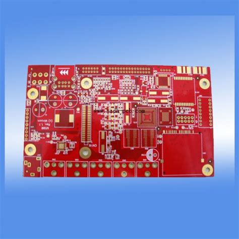
What are HDI PCBs?
HDI PCBs are printed circuit boards that feature higher wiring density per unit area compared to conventional PCBs. This is achieved through the use of smaller vias, finer trace widths and spaces, and advanced manufacturing techniques. HDI PCBs allow for the integration of more components and functionality into a smaller footprint, making them ideal for compact, high-performance electronic devices.
The IPC (Association Connecting Electronics Industries) defines HDI PCBs as having one or more of the following attributes:
- Via diameter less than 150 microns (0.15 mm)
- Line width and spacing less than 100 microns (0.1 mm)
- Capture pad diameter less than 400 microns (0.4 mm)
Benefits of HDI PCBs
HDI PCBs offer several advantages over traditional PCBs, including:
-
Miniaturization: HDI PCBs enable the creation of smaller, more compact electronic devices by allowing more components to be placed in a smaller area.
-
Improved electrical performance: The shorter signal paths and reduced layer count in HDI PCBs result in improved signal integrity, reduced crosstalk, and faster signal propagation.
-
Increased functionality: With the ability to incorporate more components and features, HDI PCBs enable the development of more sophisticated and feature-rich electronic devices.
-
Reduced weight: The compact nature of HDI PCBs contributes to overall device weight reduction, which is particularly important for portable and aerospace applications.
-
Cost-effectiveness: Although HDI PCBs may have higher initial manufacturing costs, they often lead to cost savings in the long run due to reduced assembly time, fewer components, and improved yield rates.

HDI PCB Manufacturing Processes
HDI PCBs require advanced manufacturing processes to achieve their high-density characteristics. Some of the key processes involved in HDI PCB manufacturing include:
1. Microvias
Microvias are small, laser-drilled holes that connect the outer layer to the inner layers of an HDI PCB. They have a diameter less than 150 microns and are typically formed using laser ablation or photo-imaging techniques. Microvias enable higher routing density and improved signal integrity by reducing the distance between layers.
2. Sequential Lamination
Sequential lamination is a process in which additional layers are added to an already fabricated PCB. This allows for the creation of complex, multi-layer HDI PCBs with buried and blind vias. Sequential lamination enables the manufacturing of PCBs with higher layer counts and increased functionality.
3. Buried and Blind Vias
Buried vias are used to connect inner layers of an HDI PCB without penetrating the outer layers. Blind vias, on the other hand, connect an outer layer to one or more inner layers but do not penetrate through the entire board. The use of buried and blind vias allows for greater routing flexibility and higher component density.
4. Fine Line Patterning
HDI PCBs require fine line patterning to achieve the narrow trace widths and spaces necessary for high-density designs. This is typically accomplished using advanced photolithography techniques and high-resolution imaging systems.

HDI PCB Design Considerations
Designing HDI PCBs requires careful consideration of several factors to ensure optimal performance and manufacturability. Some key design considerations include:
-
Signal integrity: HDI PCBs must be designed with signal integrity in mind, taking into account factors such as impedance control, crosstalk, and electromagnetic interference (EMI).
-
Thermal management: With higher component density comes increased heat generation. HDI PCBs must be designed with proper thermal management techniques, such as the use of thermal vias and heat spreaders, to ensure reliable operation.
-
Manufacturing constraints: Designers must work closely with PCB manufacturers to ensure that their designs are compatible with the chosen manufacturing processes and can be produced reliably and cost-effectively.
-
Testing and inspection: HDI PCBs require specialized testing and inspection techniques due to their high-density nature. Designers should incorporate appropriate test points and design for testability to facilitate the manufacturing process.

Applications of HDI PCBs
HDI PCBs find applications in a wide range of industries and products, including:
-
Consumer electronics: Smartphones, tablets, wearables, and other compact consumer devices rely heavily on HDI PCBs to achieve their small form factors and advanced functionality.
-
Aerospace and defense: HDI PCBs are used in avionics, satellite systems, and military equipment, where reliability, performance, and weight reduction are critical.
-
Medical devices: Implantable devices, diagnostic equipment, and other medical electronics benefit from the miniaturization and improved functionality enabled by HDI PCBs.
-
Automotive: As vehicles become more electronic-dependent, HDI PCBs are increasingly used in advanced driver assistance systems (ADAS), infotainment systems, and other automotive applications.
-
Industrial automation: HDI PCBs are used in sensors, controllers, and other industrial automation components, where high performance and reliability are essential.
HDI PCB Market and Future Trends
The global HDI PCB market is expected to grow significantly in the coming years, driven by the increasing demand for compact, high-performance electronic devices across various industries. According to a report by Grand View Research, the global HDI PCB market size was valued at USD 10.3 billion in 2020 and is expected to expand at a compound annual growth rate (CAGR) of 11.2% from 2021 to 2028.
Several trends are shaping the future of HDI PCBs, including:
-
5G technology: The adoption of 5G networks is expected to drive the demand for HDI PCBs in smartphones, base stations, and other 5G-enabled devices.
-
Internet of Things (IoT): The proliferation of IoT devices, which often require compact, high-performance electronics, is expected to fuel the growth of the HDI PCB market.
-
Flexible and rigid-flex HDI PCBs: The increasing demand for wearables and other flexible electronics is driving the development of flexible and rigid-flex HDI PCBs.
-
Advanced materials: The use of advanced materials, such as low-loss dielectrics and high-performance laminates, is expected to improve the performance and reliability of HDI PCBs.
Frequently Asked Questions (FAQ)
-
What is the difference between HDI PCBs and conventional PCBs?
HDI PCBs have higher wiring density per unit area compared to conventional PCBs, achieved through smaller vias, finer trace widths and spaces, and advanced manufacturing techniques. This allows for the integration of more components and functionality into a smaller footprint. -
What are the benefits of using HDI PCBs in electronic devices?
The benefits of using HDI PCBs include miniaturization, improved electrical performance, increased functionality, reduced weight, and cost-effectiveness in the long run. -
What are microvias, and how do they contribute to HDI PCB performance?
Microvias are small, laser-drilled holes that connect the outer layer to the inner layers of an HDI PCB. They have a diameter less than 150 microns and enable higher routing density and improved signal integrity by reducing the distance between layers. -
What industries commonly use HDI PCBs?
HDI PCBs are commonly used in consumer electronics, aerospace and defense, medical devices, automotive, and industrial automation industries. -
What are some future trends in the HDI PCB market?
Future trends in the HDI PCB market include the adoption of 5G technology, the proliferation of IoT devices, the development of flexible and rigid-flex HDI PCBs, and the use of advanced materials to improve performance and reliability.
| Parameter | Conventional PCBs | HDI PCBs |
|---|---|---|
| Via Diameter | > 150 microns | < 150 microns |
| Line Width and Spacing | > 100 microns | < 100 microns |
| Capture Pad Diameter | > 400 microns | < 400 microns |
| Layer Count | Typically lower | Can be higher |
| Component Density | Lower | Higher |
| Signal Integrity | Good | Excellent |
| Applications | General electronics | High-performance, compact devices |
In conclusion, HDI PCBs have become an essential component in the design and manufacturing of modern, high-performance electronic devices. Their ability to enable miniaturization, improve electrical performance, and increase functionality has made them indispensable across various industries. As technology continues to advance and consumer demands evolve, the HDI PCB market is expected to grow significantly, driven by trends such as 5G technology, IoT, and the development of flexible and rigid-flex HDI PCBs. By understanding the benefits, manufacturing processes, design considerations, and applications of HDI PCBs, engineers and manufacturers can leverage this technology to create innovative, reliable, and compact electronic devices that meet the needs of today’s rapidly evolving market.
Leave a Reply